|
|
|
|
http://www.tms.org/pubs/journals/JOM/0006/Slaughter/Slaughter-0006.html
|
|
Materials for Magnetic Memory: Overview
|
|
|
|
http://www.tms.org/pubs/journals/JOM/0006/Slaughter/Slaughter-0006.html
|
|
|
TABLE OF CONTENTS |
|---|
|
|
Recent advances in magnetic tunnel junction material are driving the development of magnetoresistive random access memory with attributes that are competitive with semiconductor memory. The large magnetoresistance signal of this material enables fast memory-read operations. In addition, the memory is nonvolatile (the information remains stored when the power is turned off) because the information is stored in the magnetic state of the bit. The large signal also makes magnetic tunnel junction material an attractive candidate for magnetic-media read heads and other types of sensor applications.
Since 1971, anisotropic magnetoresistive (AMR) Ni-Fe alloy
thin films have been explored for use in magnetic field sensing.1
These types of ferromagnetic thin films change resistance depending on the relative
direction between film magnetization and in-plane current direction. Although
the total signal change or magnetoresistance (MR) ratio, expressed as the change
in resistance divided by the minimum resistance, is typically two percent for
Ni-19Fe alloy, its field sensitivity is much larger than that obtained through
coil winding. Unlike inductive magnetic field sensors, the AMR sensor is speed
independent. Devices using this type of material include read heads in high-density
hard disk drives, magnetic field sensors for a variety of applications, and
magnetoresistive random access memory (MRAM).
In 1988, a new type of magnetoresistive material, termed giant magnetoresistance
(GMR) material, was discovered.2,3
The material is made of at least two magnetic layers separated by a conducting
interlayer. Its resistance depends on the relative orientation between the neighboring
magnetic layers. It is a maximum when the directions are antiparallel and a
minimum when they are parallel. The MR ratio is 6-15% for a simple structure
with two magnetic layers and up to 80% for an antiferromagnetically coupled
multilayer. The strong antiferromagnetic (AF) exchange coupling seen in some
multilayers forces adjacent layers to be antiparallel and is usually avoided
in applications. Without the AF exchange coupling, typically MR is 6-20% for
weakly coupled GMR films with two to three magnetic layers. Due to its improved
signal compared to AMR material, GMR films result in enhanced device performance
in most applications. GMR films have already been incorporated into commercial
read heads, and development for other device applications, such as sensors and
MRAM, is underway. The GMR films are most often used with current flowing in
the film plane. The resistance of devices using current perpendicular to the
film plane is very low, thus limiting their application potential for current-generation
microelectronic lithography dimensions.
In the early 1990s, high MR was discovered for magnetic tunnel junction (MTJ)
material.4,5
MTJ material is made of at least two magnetic layers separated by an insulating
tunnel barrier. The current flows perpendicular to the film plane, and the best
results have been achieved with aluminum-oxide tunnel barriers. Since the initial
experimental discovery of MTJ material with promising MR, the technique of producing
these materials, as well as key properties, has been dramatically improved.6,7
Tunneling MR values are now widely reported are in the 20-50% range, much higher
than typical GMR films. The tunneling resistance depends exponentially on the
tunnel-barrier thickness and is measured by the resistance-area (RA) product.
Early work reported quite high values of RA, often in the GW-mm2
range, but recent work has shown good MR down to the 10 W-mm2
range. The current RA value of MTJ material is ideal for MRAM and sensor applications,
but is still high for magnetic-recording read head applications.
The basic concept of MRAM uses magnetization direction as information storage
and the resultant resistance difference for information readout. The development
of MRAM began approximately ten years ago in response to the need for a durable,
radiation-hard, nonvolatile RAM.8
The potential of the technology has improved dramatically with each advance
in magnetic materials. The first material used was AMR Ni-Fe-Co/Ta-N/Ni-Fe-Co
sandwich films. The MR ratio was limited to 2%, and the actual MR used in memory
states was only about 0.5%. The low signal was responsible for the relatively
slow read-access time of around 250 ns. The critical dimension of the cell was
larger than 1 mm, which lagged behind semiconductor
memories by many generations. Such memory technology is very attractive for
niche markets such as space applications, but it is not competitive with general
semiconductor memories in speed, density, and cost.
The discovery of the GMR effect was a boost to MRAM technology. Not only is
the signal strength larger, but the characteristics of the physical phenomenon
itself are well suited for MRAM, which uses magnetic-moment direction as information
storage and the resultant MR difference for sensing. A submicrometer critical
dimension of the MRAM cell is essential for its competitiveness in the general
memory market.
A number of different memory-storage methods using different types of GMR films
have been explored for application in high-density memory.9,10
Since the sheet resistance of the GMR film is small compared to that of a complementary
metal-oxide semiconductor (CMOS) transistor, a number of GMR MRAM memory cells
must be connected in series with a CMOS transistor, so that total resistance
from the memory cells is much larger than that from the transistor. Although
good from a design point of view, this scheme effectively decreases the usable
signal, making it difficult to design a high-speed memory.
MTJ material is quickly finding applications in MRAM and magnetic-field sensing.11,12
Major advantages of MTJ material include a larger signal, from 20-50% depending
on the polarization of the magnetic electrodes used, and its tunable RA, depending
on barrier thickness and degree of oxidation. It is possible to make MTJ memory
cells with one cell in series with a minimum-size silicon CMOS transistor for
isolation. This kind of high-density architecture is suitable for fast-speed,
low-power memory applications.12
 |
|
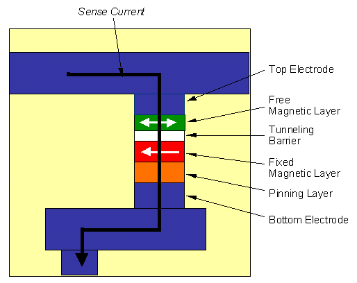
Figure 1. A schematic of an MTJ memory cell. Arrows indicate possible directions of magnetic movement. |
The layers of the MTJ stack are formed by sputter-deposition techniques with
deposition rates in the �ngstrom-per-second range. Two such techniques have
been applied successfully--physical vapor deposition, specifically planar magnetron
sputtering, and ion-beam deposition. The tools and techniques used for the metal-layer
deposition are the same as those used for GMR films.14,15
The best methods for producing the insulating tunnel barrier are not yet clear;
various techniques are currently under study throughout the world. The best
results to date are for AlOx tunnel-barrier layers made by depositing a metallic
aluminum layer, between 5 � and 15 � thick, and then oxidizing it by one of
several methods. We have studied several types of plasma oxidation16
as well as oxidation in air and ion-beam oxidation. Additional techniques studied
by other groups include oxidation by glow-discharge plasma,5
atomic-oxygen exposure, and ultraviolet-stimulated O2
exposure.17
The necessity of controlling the magnetic properties of the magnetic layers
introduces special requirements on the deposition process. For example, most
ferromagnetic materials have an inherent magnetic anisotropy that is related
to ordering on an atomic scale.18
The direction of this anisotropy can be set during the deposition of the layer
by applying a magnetic field across the wafer. The resulting uniaxial anisotropy
is observed as magnetic easy and hard directions in the magnetization of the
layer. Since the anisotropy axis affects the switching behavior of the material,
the deposition system must be capable of projecting a uniform magnetic field
across the wafer, typically in the 20-100 Oe range, during deposition. Other
magnetic properties, such as coercivity and magnetorestriction, also are dependent
on the deposition process and must be controlled by the choice of magnetic alloy
and deposition conditions. Because the switching field of a patterned bit depends
directly on the thickness of the free layer, the requirements for thickness
uniformity and repeatability are strict. A total combined variation of less
than 2% will be needed. These tolerances are currently met by R&D deposition
tools, but are not standard for semiconductor production tools.
MTJ material cannot be tested in blanket form. Since the current must pass perpendicular
to the layers, it must be patterned so that the top and bottom electrodes can
be separately contacted. In addition, one must be careful about the resistance
of the electrodes, even in a four-point probe measurement, since current-distribution
effects can produce erroneous results when the junction resistance is low.19
 |
|
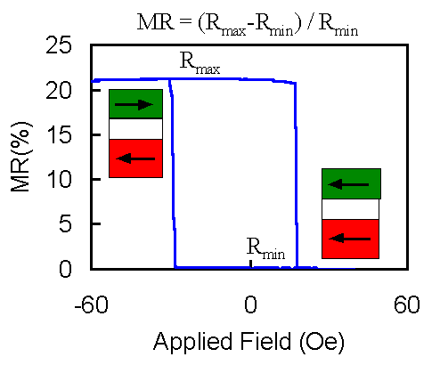
Figure 2. An MR curve for an MTJ bit. The resistance is low/high when the polarization of the magnetic layers is parallel/antiparallel. |
For the material studies presented here, standard contact lithography techniques
were used to form 300 mm �
100 mm rectangular junctions. Testing was done using
a four-point electrical prober. One set of the current and voltage probes was
placed on pads in contact with one MTJ electrode, and the other set of probes
was contacted to the other electrode. An external field was applied, and field
versus resistance of MTJ was measured. The MR was then extracted from these
measurements; a typical MR loop is shown in Figure
2. Bottom and top electrodes of 400 � thick aluminum were used to provide
low-resistance contacts to the junctions. For the study of small bits, a multimask
process with deep ultraviolet lithography was used.
For a submicrometer-patterned MTJ device to have a resistance that is suitable
for MRAM, the tunnel-barrier thickness must be on the order of 20 � or less.
In addition to being pinhole free and very smooth, the AlOx tunneling barrier
must be extremely uniform over a wafer. Since the resistance of the junction
is exponentially dependent on thickness, small variations in the AlOx thickness
result in large variations in the resistance.16
The uniformity and absolute values of the resistance, in addition to the MR
values of the cells, are important parameters for the read operation, since
in preferred architecture the cell signal, which depends on cell resistance
and MR, is compared with a nearby reference cell during read operation.
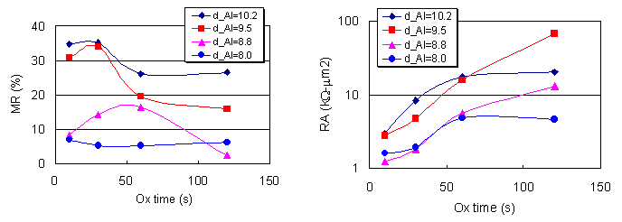
MR values above 30% for RA in the 1-1,000 kW-mm2
range have been obtained by optimizing aluminum thickness and oxidation time.
Figure 3 illustrates the behavior of
MR and the RA product for MTJ material with Ni-Fe alloy electrodes. For aluminum
thickness above 9 �, MR peaks at 35% with an RA in the 1-10 kW-mm2
range as desired for the MRAM elements. The peak indicates that either over-oxidizing
or under-oxidizing the aluminum reduces MR. Over-oxidizing results in oxidation
of the magnetic electrode beneath the barrier, while under-oxidizing leaves
metallic aluminum at that bottom interface. For the series of samples shown
in the figure, MR drops abruptly for aluminum thickness (dAl)
below 9 �, probably due to roughness at the tunnel-barrier interfaces that leads
to partial shorts or tunneling hot spots. The RA increases exponentially with
plasma oxidation time in the region of the best MR. Studies of varying dAl
with constant oxidation time also exhibit exponentially increasing RA with dAl
in the region of best MR. Because of the exponential dependence on both aluminum
thickness and oxidation time, producing MTJ material with good resistance uniformity
over an entire wafer is challenging. However, with excellent aluminum thickness
uniformity, RA uniformity of 10% 1-sigma over a 150 mm wafer can be routinely
obtained.
|
 |
|
|
|
|
|
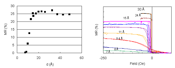
| Figure 3. The (left) MR and (right) RA product for MTJ material with Ni-Fe alloy electrodes showing the dependence on plasma oxidation time and aluminum thickness before oxidation. | Figure 4. (left) The dependence of MR on thickness of the Ni-Fe free layer for bottom-pinned MTJ material. (right) Hysterisis loops for free layers with thickness as labeled. | |
|
|
|
A thin, free magnetic layer is desirable to obtain low switching fields in patterned bits. However, there are fundamental limits on how thin it can be made. Figure 4 shows how tunneling MR depends on the free-layer thickness for MTJ material with Ni-Fe alloy electrodes. These data indicate a transition from ferromagnetic to superparamagnetic behavior for dNiFe below 15 �. Further analysis shows that these hysteresis curves are consistent with the growth of small Ni-Fe islands on the AlOx tunnel barrier that coalesce at a Ni-Fe coverage near 9 �.
 |
|
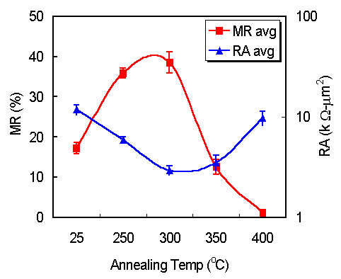
Figure 5. The effect of annealing on the MR and RA of MTJ material. |
The difference between as-deposited and low-temperature (T < 300�C) annealed
material is dramatic. Typically, MR increases significantly and resistance decreases
slightly after a low-temperature anneal, as shown in Figure
5. At temperatures above 300�C, MR degrades as resistance increases. Each
data point in the figure represents the average of about ten die across a wafer.
Clearly, there are changes occurring in the tunnel barrier or interfaces with
the barrier that strongly impact the properties of the spin-dependent tunneling.
The practical implications of this behavior are described under Status
and Challenges.
To better understand the changes that occur near the interfaces in the tunnel
junction during the initial low-temperature anneal, x-ray photoelectron spectroscopy
experiments were performed on simplified structures. Samples consisting of typical
bottom electrode layers covered by AlOx were inserted into an ultrahigh vacuum
chamber for annealing and x-ray photoelectron spectroscopy analysis using a
magnesium-anode x-ray source and a double-pass cylindrical-mirror electron energy
analyzer. Changes occurred in the photoelectron peaks corresponding to the Fe
2p1/2 and 2p3/2 levels when one sample was annealed at 250�C and 300�C. A large
shoulder on the right side of the 2p1/2 peak was observed and correlated to
the presence of oxidized iron in the vicinity of the AlOx barrier. The chemical
state of the iron oxide is unknown, but the peak shift was similar to FeO rather
than Fe2O3.
On annealing at 250�C, the FeOx signal was lower, and after the 300�C anneal
it was lower still. These results imply that some of the iron is oxidized together
with the aluminum layer, but is at least partially reduced again to metallic
iron when annealed. The initial state may be due to intermixing of iron and
aluminum when the aluminum is deposited. The intermixed iron is then oxidized
with the aluminum, giving rise to the large FeOx peak. Since the enthalpy of
formation of aluminum oxide is larger (more negative) than iron oxide, the reduction
effect could be due to a competition between the iron and aluminum for the available
oxygen, which favors the aluminum.12,20
Understanding the properties of thin magnetic films is essential to engineering
a reliable device. Characterizing how the magnetic layers react to deposition,
seed layers, thermal anneal, operating temperature, and stress is important
to ensure that these thin layers will withstand the rigors of processing, packaging,
and operation. The permutations of magnetic layer and seed, deposition technique,
thermal anneal, stress, etc. lead to a large number of structures to be investigated.
A summary of magnetic properties and characterization is beyond the scope of
this article, but this section focuses on one experiment that illustrates the
type of issues and characterization techniques encountered. This experiment
involves using Pt-Mn to pin the magnetization direction of Ni-Fe.
A ferromagnetic thin film is pinned when placed in contact with an AF thin film.
For an uncoupled, free, ferromagnetic film, the magnetic orientation of the
film displays a hysteretic behavior pointing in the direction of the last applied
saturating field. If a saturating field is applied and then taken away, the
magnetic orientation of this free film will be in the direction of that field.
If the direction of the applied saturating field is reversed and again taken
away, the magnetic orientation of the film will be reversed. Thus, in zero applied
field, either orientation is possible. A ferromagnetic film pinned by an AF
layer displays similar behavior, but has an offset. In zero field, the ferrromagnetic
film will align in one direction. An exchange coupling between the ferromagnetic
and AF layers, at their mutual interface, causes the ferromagnetic layer to
be preferentially aligned in one direction. For our memory devices, this preferential
alignment or pinning is used to lock one layer in a fixed direction. Much of
our work on AF pinning materials, and of others in the field, has revolved around
manganese-based antiferromagnetic materials such as Pt-Mn, Ir-Mn, Rh-Mn, and
Fe-Mn.
 |
|
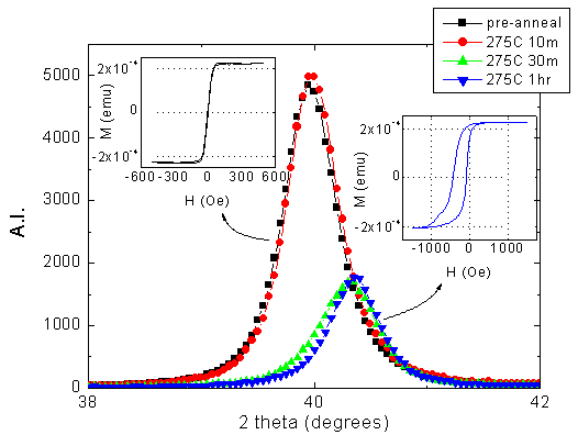
Figure 6. The annealing behavior of a thin film stack: Ta(50 �)/Ni-Fe(30 �)/Pt-Mn(300 �)/Ni-Fe(60 �)/Ta(100 �). The main figure shows the evolution of the q-2q x-ray diffraction spectrum as the (111) oriented f.c.c. Pt-Mn transforms to f.c.t. Pt-Mn during anneal. The insets show the corresponding change in the M-H loop of the Ni-Fe when the antiferromagnetic f.c.t. Pt-Mn exchange couples to it. |
 |
|
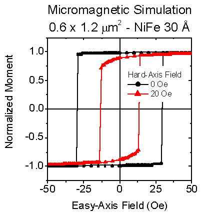
Figure 7. Calculated hysteresis curves for a 0.6 � 1.2 mm2 bit with 0 Oe and 20 Oe hard-axis fields applied. |
Pt-Mn is a particularly interesting pinning material because it remains AF at relatively high temperatures. Unlike many of the commonly used AF alloys, as-deposited Pt-Mn is not AF. Instead, this material must be post annealed, resulting in a phase transformation from face-centered cubic (f.c.c.) to a face-centered tetragonal (f.c.t.) crystal structure. The f.c.t. phase of Pt-Mn is AF and will pin an adjacent ferromagnetic film. This behavior is shown in Figure 6. This figure displays x-ray and magnetic characterization of a Ni-Fe ferromagnetic layer pinned by a Pt-Mn AF layer. In the x-ray diffraction data, the phase transformation to f.c.t. from f.c.c is clearly seen to occur between a ten minute and 30 minute anneal at 275�C. The inset magnetic hysteresis loops (magnetization vs. applied field) show how the pinning strength increases accordingly with annealing time. The shift and broadening of the Ni-Fe hysteresis loop in the annealed material is characteristic of a pinned ferromagnetic film. Once pinned, the exchange bias causes the magnetic orientation of the film to be in one direction at zero applied field. The data shown here are for only one thickness of Pt-Mn, one thickness of surrounding Ni-Fe layers, and a seed layer of tantalum. Other layer thicknesses and seed layers can produce a variety of different results.
Understanding and controlling the micromagnetic behavior of MTJ elements is
essential for reproducible and reliable switching characteristics.21,22
The switching field is mainly governed by the magnetic-shape anisotropy that
arises from the element boundaries. Hence, bit size, shape, and aspect ratio
all play roles in controlling the micromagnetic arrangement and, therefore,
the switching behavior.
Ideally, bits with a single magnetic domain would coherently rotate in response
to the selecting and switching fields in an MRAM device. In real elements, the
magnetic configuration is complicated by the presence of edges and is not single-domain
in the ideal sense. Therefore, switching is strongly dependent on the details
of the patterned shape.
Micromagnetic simulations23
of single-element switching behavior have been performed. Figure
7 is a plot of the calculated hysteresis curves for a 0.6 mm2
� 1.2 mm2
ellipse with 0 Oe and 20 Oe hard-axis select fields. The predicted behavior
is in excellent agreement with the experimental measurements of real devices.
Figure 8 shows a vector representation
of the micromagnetic structure of this element during the switching transition
with zero applied hard-axis field. The curling of the end domains is evident
at the start of the transition. The reversal begins at the ends and sweeps through
the body of the element, giving a crisp transition in the hysteresis curve.
|
|
 |
|
Figure 8. Vector representation of the micromagnetic behavior during a switching transition with zero applied hard-axis field. (from top to bottom) -29 Oe easy-axis field immediately before transition; transition wall sweeps through element; and -30 Oe easy-axis field immediately after switch. |
 |
|
|
We have successfully integrated MTJ-based MRAM bits with CMOS in a fully fabricated
256 � 2 test vehicle in which the MTJ memory cells
were inserted into the back end of a 0.6 mm CMOS
process. The read-address access time is 14 ns, and the read-cycle time is 24
ns, consuming 800 mA of current at 3 V operation
at room temperature. The program access time is 14 ns. This performance is very
encouraging for 0.6 mm technology and is anticipated
to improve significantly at smaller lithography dimensions. These results indicate
that MRAM has the potential to be a competitive memory with the attributes of
high-speed read and write, as well as nonvolatility.
One of the challenges involved in the integration of MRAM technology is temperature
compatibility with the CMOS process. Several standard CMOS process steps occur
at or above 400�C. As shown in Figure 5,
the MR of typical MTJ material begins to degrade at temperatures above 300�C
and drops sharply by 400�C. Thus, for a working memory either the MTJ material
must be improved to withstand these standard process temperatures, or low-temperature
processes must be developed for MRAM technology.12
For our demonstration circuits, special low-temperature processes were used
to prevent the MTJ material from being exposed to higher temperatures during
MRAM processing. Improvements in the thermal endurance that would make the materials
compatible with standard processes would enhance the manufacturability of the
technology.
Obtaining very uniform RA over large wafers is another challenge. Techniques
that have been explored include forming the aluminum-oxide tunnel barrier with
air; reactive sputtering; plasma oxidation with plasma source; plasma oxidation
with power introduced from the target side; and plasma oxidation with power
introduced from the substrate side.16
The results show that all techniques can be made to work. Plasma oxidation is
favored due to its simplicity and manufacturing compatibility. It was also discovered
that different oxidation methods used in this study caused little difference
in MTJ resistance uniformity. The latter is mainly determined by the aluminum
metal thickness uniformity. Modeling based on Simmons' theory supports the experimental
finding. This illustrates that the key to better MTJ RA uniformity is to improve
the aluminum metal layer thickness uniformity.
A final challenge is producing MTJ material with very low RA. As bit sizes are
reduced, MRAM may require material with lower RA. In addition, use in hard-disk
read heads would require a much lower resistance for the first generation of
product. Obtaining a thinner tunnel barrier without losing MR is one of the
key factors to achieving low RA. The MR loop shown in Figure
2 is for an MTJ structure with only 0.7 nm of aluminum oxidized to form
the tunnel barrier. Its RA is only 480 W-mm2.
This low RA value is appropriate for future generations of MRAM and close to
the range that will be useful for read heads.
This work was partially supported by the U.S. Defense Advanced Research Projects Agency.
1. R.P. Hunt,
"A Magnetoresistive Read Out Transducer," IEEE
Trans. Mag., (1971), pp. 150-154.
2. M.N. Baibich et al., Phys.
Rev. Lett., 61 (1988), p. 2472.
3. H. Sato et al., "Galvanomagnetic
Properties of Ag/M (M = Fe,Ni,Co) Layered Metallic Films," Superlattices
and Microstructures, 4 (1988), pp. 45-50.
4. T. Miyazaki and N. Tezuka,
"Giant Magentic Tunneling Effect in Fe/Al2O3/Fe Junction," J.
Magn. Magn. Mater., 139 (1995), p. L231.
5. J.S. Moodera et al., "Large
Magnetoresistance at Room Temperature in Ferromagnetic Thin Film Tunnel Junctions,"
Phys. Rev, Lett.,
74 (1995), pp. 3273-3276; J.S. Moodera and L.R. Kinider, J.
Appl. Phys., 79 (1996), p. 4724.
6. S.S.P. Parkin, R.E. Fontana,
and A.C. Marley, J.
Appl. Phys., 81 (1997), p. 5521.
7. R.C. Sousa et al., "Large
Tunneling Magnetoresistance Enhancement by Thermal Anneal," Appl.
Phys. Lett., 73 (1998), pp. 3288-3290.
8. J.M. Daughton, "Magnetoresistive
Memory Technology," Thin
Solid Films, 216 (1992), pp. 162-168.
9. E.Y. Chen et al., J.
Appl. Phys., 81 (1997), p. 3992.
10. S. Tehrani et al., "High
Density Submicron Magnetoresistive Random Access Memory," J.
Appl. Phys., 85 (1999), pp. 5822-5827.
11. S.S. P. Parkin et al.,
"Exchange-Biased Magnetic Tunnel Junctions and Application to Non-Volatile Magnetic
Random Access Memory," J.
Appl. Phys., 85 (1999), p. 3741.
12. S. Tehrani et al., "Progress
and Outlook for MRAM Technology," IEEE
Trans. Mag., 35 (2000), pp. 2814-2819; and S. Tehrani, B. Engel, J.M.
Slaughter, E. Chen, M. DeHerrera, M. Durlam, P. Naji, R. Whig, J. Janesky, and
J. Calder "Recent Developments in Magnetic Tunnel Junction MRAM,"
IEEE
Trans. Mag. (in press).
13. J.M. de Teresa et al.,
"Inverse Tunnel Magnetoresistance in Co/SrTiO3/La0.7/Sr0.3/MnO3: New Ideas on
Spin-polarized Tunneling," Phys.
Rev. Lett., 82 (1999), pp. 4288-4291.
14. J.M. Slaughter, E.Y. Chen,
and S. Tehrani, "Magnetoresistance of Ion-Beam Deposited Co/Cu/Co and NiFe/Co/Cu/Co/NiFe
Spin Valves," J. Appl.
Phys., 85 (1999), pp. 4451-4453.
15. W.F. Egelhoff, Jr., et
al., J. Appl. Phys.,
79 (1996), p. 5277.
16. E.Y. Chen et al., "Comparison
of Oxidation Methods for Magnetic Tunnel Junction Material," J.
Appl. Phys., 87 (April 2000).
17. H. Boeve et al., "Strongly
Reduced Bias Dependence in Spin-Tunnel Junctions Obtained by Ultraviolet Light
Assisted Oxidation," Appl.
Phys. Lett., 76 (2000), pp. 1048-1050.
18. R.M. Bozorth, Ferromagnetism
(New York: D. van Nostrand, 1951).
19. J.S.
Moodera et al., Appl.
Phys. Lett., 69 (12996), p. 708.
20. David J. Keavney et al.,
unpublished material.
21. J. Shi et al., "End Domain
States and Magnetization Reversal in Submicron Magnetic Structures" IEEE
Trans. Mag., 34 (1998), p. 997.
22. J. Shi et al., "Magnetization
Vortices and Anomalous Switching in Patterned NiFeCo Submicron Arrays," Appl.
Phys. Lett., 74 (1999), pp. 2525-2527.
23. LLG Micromagnetics SimulatorTM,
Tempe, Arizona.
J.M. Slaughter, E.Y. Chen, R. Whig, B.N. Engel, J. Janesky, and S. Tehrani are with Motorola Labs, Physical Sciences Research Laboratories.
For more information, contact J.M. Slaughter, Motorola Labs,
MD-EL508, 2100 East Elliot Road, Tempe, Arizona 85284 (UPDATED ADDRESS: Mail
Drop ML34, Motorola Labs, 7700 South River Parkway, Tempe, Arizona 85284).
Direct questions about this or any other JOM page to jom@tms.org.
| If you would like to comment on the June
2000 issue of JOM,
simply complete the JOM on-line critique form |
|||||
|---|---|---|---|---|---|
| Search | TMS Document Center | Subscriptions | Other Hypertext Articles | JOM | TMS OnLine |