|
|
|
|
http://www.tms.org/pubs/journals/JOM/0010/Cosandey/Cosandey-0010.html
|
|
|
|
|
|
http://www.tms.org/pubs/journals/JOM/0010/Cosandey/Cosandey-0010.html
|
|
|
TABLE OF CONTENTS |
|---|
|
|
The development of gas sensor devices with optimized selectivity and sensitivity has been gaining prominence in recent years. The use of a semiconductor fabrication line is the preferred manufacturing process because of the potential to reduce cost. However, fundamental materials and processing issues, which are critical for a high-performance gas sensor, need to be addressed. Among the new technologies, a nanocrystalline material offers immense promise for improved sensitivity. This article provides a rationale for using nanocrystalline materials in gas sensors, and outlines the challenges facing commercialization of this new class of material.
In recent years, interest has grown in the development of
an electronic "nose," capable of detecting mixed gases and even odors. Instead
of analyzing all of the gas constituents by a technique such as gas chromatography,
an electronic nose looks for specific patterns or fingerprints of the gas mixture.
Such a device generally consists of 4-22 chemical sensors, each one sensitive
to a specific gas and a pattern recognition system. Various prototypes, based
on organic as well as inorganic sensing materials, have appeared in the market.
Because of their simplicity and low cost, semiconductor metal-oxide gas sensors
stand out among the ones used in multi-sensor arrays. A multi-sensor array has
been proposed for environmental monitoring,1
in which gas sensing would be based on changes in the surface or near-surface
oxide conductivity. Such conductivity changes are caused by the formation of
a space charge region induced by either gas adsorption or by the formation of
oxygen vacancies on the surface. Improved efficiency and sensing selectivity
of these devices require detailed understanding of the surface and interfacial
processes at the atomic level, and their relationship with materials properties
and device performance.
A non-exhaustive list of semiconductor oxide materials with targeted selectivity
for specific gases is shown in Table I, which lists only
materials used for air quality monitoring.
Two of the most important issues in gas sensing devices are gas sensitivity
(detection of gas concentrations at the ppm level) and gas selectivity3,15
(detection of specific gases in a mixed gas environment). Semiconductor oxides
suffer mostly from a lack of gas selectivity. For instance, the most commonly
used oxide, SnO2, can be sensitized to different
gases by judicious choice of operating temperature, microstructural modification,
and by the use of dopants and catalysts.4
Nanostructured materials present new opportunities for enhancing the properties
and performance of gas sensors because of the much higher surface-to-bulk ratio
in nanomaterials compared to coarse micrograined materials.
|
Table I. Partial List of Semiconductor Oxides with Targeted Selectivity for Specific Gases for Environmental and Air Quality Monitoring |
||
|
Oxide Type
|
Detectable Gas
|
References
|
|
|
|
|
|
SnO2
|
H2,CO,NO2,H2S,
CH4
|
|
|
TiO2
|
H2,
C2H5OH,
O2
|
|
|
Fe2O3
|
CO
|
|
|
Cr1.8Ti0.2O3
|
NH3
|
|
|
WO3
|
NO2, NH3
|
|
|
In2O3
|
O3, NO2,
|
|
|
LaFeO3
|
NO2, NOx
|
|
|
|
||
|
|
 |
|
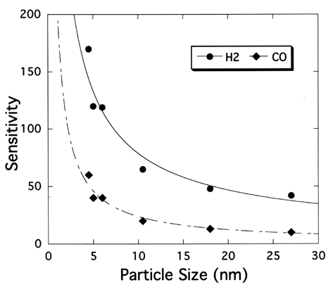
Figure 1. The effect of particle size on gas sensitivity for an SnO2 oxide sensor exposed to CO and H2 gases.15 |
|
|
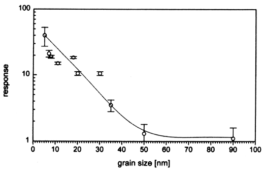
Figure 2. The effect of In2O3 grain size on sensor sensitivity to 1.0 ppm NO2 at 250�C.13 |
Establishing sensor selectivity for specific gases is difficult and challenging. Selectivity is dependent on many parameters, such as gas adsorption and co-adsorption mechanisms, surface reaction kinetics, and electron transfer to or from the conduction band of the semiconductor. At present, sensor selectivity remains, for the most part, empirical. In practice, selectivity is achieved by enhancing gas adsorption or promoting specific chemical reactions via catalytic or electronic effects using bulk dopants, surface modification methods, and by the addition of metallic clusters or oxide catalysts.3,16 For instance, the selectivity of chemical sensors can be strongly influenced by the addition of metal clusters such as platinum and palladium, resulting in an increase in the sensor selectivity to reducing gases, such as CO.17 An increase in selectivity is believed to be caused by close coupling between the sensing and catalytic properties of the metal/oxide system.
Recently studies indicate that the most noble metal, gold,
on transition metal oxides could have important applications for room-temperature
catalytic oxidation of CO to CO2 as well as
a selective gas sensor for CO and hydrogen.18-23
Other metal-oxide systems where selectivity is promoted by gold include Au-WO3
for NH3 selectivity and Au-In2O3
for ozone and trimethylamine selectivity.12
These selectivity effects are caused by a yet unknown but unique synergistic
effect between gold and the oxides TiO2, WO3,
or In2O3.
For chemical sensors, the increased selectivity due to additions of metallic
clusters is explained using two mechanisms, chemical sensitization and electronic
sensitization.12,15
In chemical sensitization, the metal particles act as centers for surface-gas
adsorption, which is then followed by spill-over onto the oxide surface to react
with the negatively charged chemisorbed oxygen. On the other hand, electronic
sensitization results in a direct electronic interaction between the oxide surface
and metal particles via metal oxidation and reduction processes. This is the
case for silver and palladium, which are known to form oxides in the presence
of oxygen. In the presence of reducing gases, the oxidized metal particles are
reduced, leading to a change in the carrier concentration of the semiconductor
oxide substrate. For gold on oxides, however, the mechanisms involved are still
not clearly understood.24
Also unknown is how chemisorption, size effects, and interactions with semiconductor
oxide substrate relate to chemical sensing.
Sensitivity is generally enhanced either by doping, which modifies the carrier
concentration and mobility, or by microstructural changes such as reduction
of the oxide particle size to the nanometer scale.25
In recent years, the sensitivity of semiconductor oxide materials has been improved
by reducing the particle size, with greatly improved properties reported for
sizes in the 5-50 nanometer range.12,15,25,26
The effect of particle size on the sensitivity of a SnO2
sensor for H2 is shown in Figure
1,15 where an order
of magnitude increase in sensitivity occurs when the particle size decreases
to below 10 nm. The critical particle size where substantial improvement is
observed depends on oxide material, dopant, and processing method. For instance,
another study showed that sensitivity for H2
can be increased tenfold by reducing the average particle size to 22 nm.26
For In2O3
a particle size effect13
starts to occur below 50 nm with an order of magnitude increase in sensitivity
for particles in the 20 nm to 30 nm range (Figure
2).
This particle size effect is due, in part, to an increase in the surface area
since, in this size range, a large fraction of the atoms (up to 50%) are present
at the surface or the interface region with structure and properties that are
different from that of the bulk. However, the main effect is associated with
the depth of the surface space charge region affected by gas adsorption in relation
to the particle size. In the low-temperature regime, conduction variations arise
from surface-controlled processes. For chemisorption of an oxidizing gas such
as O2, the molecule dissociates to O-1,
taking an electron from the lattice. As a result, a surface depletion layer
is formed leading to a decrease in near-surface conductivity. The surface depletion
layer can be expressed by the Debye length, which is defined as:
|
LD = (eoKT/noe2)1/2
|
(1)
|
|
S = DG/Go = (Dn/no)LD
|
(2)
|
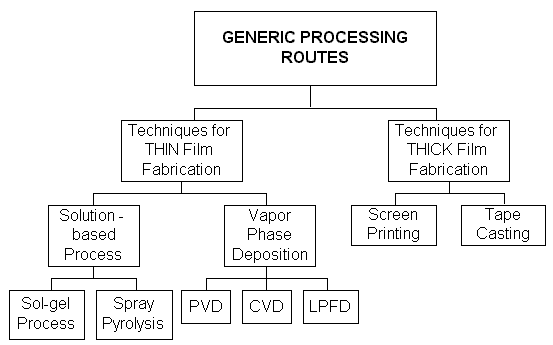
Film processing techniques fall into two categories: thin-film deposition processes
such as sputtering, evaporation, and chemical vapor condensation (CVD) for thicknesses
between 0.005 mm and 2.0 mm
and thick-film deposition processes such as screen printing and tape casting
for films thicker than 10 mm. Thermal spraying can
be used to deposit coatings of metals, ceramics, and cermets that are thicker
than ~50 mm. Figure
3 is a summary of the generic processing routes used for synthesis of gas
sensor films.
|
|
 |
|
Figure 3. A summary of the processing routes being used to fabricate thin and thick films for gas sensor applications. |
|
|
Screen printing involves printing a paste or an ink on a suitable substrate
followed by a two-stage heat treatment to form a dense (or porous) layer with
the desired structure.14,27
The paste, which consists of powders mixed with an organic medium and a binder,
should have the correct rheological properties. In addition, adherence to the
substrate and precise shrinkage characteristics are important to obtain a good
film. The technique is routinely used to deposit layers of sensor materials,
such as SnO2, TiO2,
and LaFeO3.
Recently, screen-printed pastes containing nanoparticles were deposited on 96%
alumina substrates.14,27
The "green" films were 2 mm � 2 mm and 250 mm
thick. The sensor assembly (i.e., the deposits along with the Pt-100 heating
element and interdigitated gold electrical contact) was fired in flowing N2
or air at various temperatures in the range 650-1,000�C for 1 h. After processing,
the dimensions of the films changed to 1.5 mm � 1.5
mm and 50 mm in thickness. Williams28
used SnO2 nanopowders synthesized by laser
ablation as starting materials and performed screen printing on an electrode
array. Since nanopowders produced by any of the vapor phase techniques have,
in general, a low trap density, it was not possible to avoid shrinkage cracks.
However, cracking was avoided by deliberately aggregating the particles by first
dispersing water and drying, before mixing with an a-terpineol-based
vehicle to prepare the paste. Working on similar lines, Carotta et al.29
fabricated pure and niobium-doped nanophase TiO2
films by screen printing, starting from nanopowders produced by laser pyrolysis.
Much emphasis is being placed on developing chemical solution-based thin-film
deposition technologies as an economical alternative to the more expensive chemical
vapor deposition and reactive sputtering processes. However, the quality of
the films produced by vapor deposition processes has always remained superior.
Spray pyrolysis, using an atomizing nozzle as small as 300 mm,
has been used recently to deposit SnO2 films
that were 50-300 nm thick. Tin chloride was dissolved in ethanol or deionized
water and sprayed at a deposition temperature in the range 300-550�C. Manipulation
of the structure of the films was made possible by controlling the deposition
parameters precisely.
Recognizing the usefulness of a porous film for gas sensing, Mukhopadhyay et
al.30 have developed
a modified chemical solution-based technique, where a thin adherent film of
tin sulfide is formed on a ceramic substrate by reacting sodium sulfide and
tin chloride. Subsequently, the tin sulfide film was reacted in air to produce
SnO2.
Variations of CVD techniques, such as plasma-enhanced (PECVD)31
and atmospheric-pressure (APCVD) CVD32
have been used to produce both nanopowders and nanostructured thin films. In
addition, physical vapor deposition (PVD) techniques using either an evaporation
or a sputter source have also been used extensively.7,33
In our work,34 we have
used a vapor-phase process to directly deposit, in one step, a nanostructured
film of gas sensor materials, such as SnO2
and TiO2. The process, called low-pressure
flame deposition (LPFD), is based on the combustion flame-chemical-vapor condensation
process used to produce oxide nanoparticles with minimal aggregation. Both of
these processes use a similar experimental configuration. A flat flame burner
that can be operated at low pressures of 100 torr is placed parallel to a substrate
in a stagnant flow configuration. Under these conditions, the chemical composition,
temperature, and residence time are the same across the entire surface of the
burner. When the nanoparticles that are formed in the flame are partially quenched,
a film develops on the substrate. The nanostructured film is generally porous,
although dense films have also been obtained under certain operating conditions.
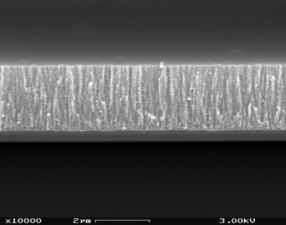
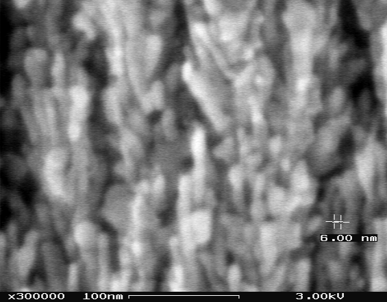
A high-resolution scanning electron microscopy image of a porous SnO2
deposited on a pre-oxidized silicon substrate is shown in Figure 4. The low-magnification
Figure 4a reveals the uniformity of
a 2.4 micrometer thick film while the high-magnification Figure
4b shows the porous nature of the LPFD films with particle sizes in the
6 nm to 20 nm range.
|
|
||
 |
 |
|
|
Figure 4. A high-resolution scanning electron microscopy image of a porous SnO2 deposit on a pre-oxidized silicon substrate at both (a) low and (b) high magnifications. |
||
|
|
||
The mechanism of film deposition in the LPFD process differs from conventional CVD in two major respects: nanoparticles are deposited on the substrate rather than the precursor being decomposed on a heated substrate and the size of the deposition area corresponds to the size of the burner. Thus, LPFD is a one-step process suitable for the formation of both thin and thick films and eliminates the need for powder processing. It is also a high-rate process, with deposition rates exceeding 1 mm/min.
Nanostructured materials are recognized as essential for achieving high gas
sensitivity. Numerous processing schemes have been tested successfully, albeit
only on a laboratory scale. Processing techniques should be able to provide
the desired oxide composition with specific dopant and requiring the least number
of processing steps. For this, vapor-based processes seem to be the most promising
approach. However, new precursors will be required for synthesizing multi-component
oxides with specific dopants. Future trends in sensor miniaturization and integration
with electronics will require processing compatibility with silicon-based technologies.
In addition to processing nanostructured oxides, more fundamental work is needed
to understand the role of nanostructured oxide materials on gas adsorption and
conductivity.
An area where greater improvements are necessary is gas selectivity. At present,
a fundamental understanding of the basic phenomena associated with metal-oxide
interaction in relation to chemical selectivity is lacking. Most of the developments
on chemical selectivity have been empirical, and further progress in this area
is not possible without an understanding of the processes and interfacial phenomena
at the atomic level. Oxide materials currently in use could be made more sensitive
by the introduction of dopants with unique gas adsorption characteristics and
by the development of new materials having specific catalytic properties for
enhancing gas selectivity.
1. G. Martinelli
et al., "Thick-Film Gas Based Nano-Sized Semiconducting Oxide Powders," MRS
Bulletin (June 1999), pp. 30-36.
2. A.M. Azad et al., "Solid-State
Gas Sensors: A Review," J.
Electrochem. Soc., 139 (1992), pp. 3690-3704.
3. W. Gopel, "New Material and
Transducers for Chemical Sensors," Sensors
and Actuators B, 18-19 (1994), pp. 1-21.
4. G. Sberveglieri, "Recent
Developments in Semiconducting Thin-Film Gas Sensors," Sensors
and Actuator B, 23 (1995), pp. 103-109.
5. L.D. Birkefeld et al., "Carbon
Monoxide and Hydrogen Detection by Anatase Modification of Titanium Dioxide,"
J. Am. Ceram. Soc.,
75 (1992), pp. 2964-2968.
6. H. Tang et al., "TiO2
Anatase Thin Films as Gas Sensors," Sensors
and Actuators B, 26-27 (1995), pp. 71-75.
7. F. Edelman et al., "E-Gun
Sputtered and Reactive Ion Sputtered TiO2
Thin Films for Gas Sensors," Inst. Electron Technol., 33 (2000), pp.
89-107.
8. T. Kobayashi et al., "Thin
Films of Supported Gold Catalysts for CO Detection," Sensors
and Actuators B, 1 (1990), pp. 222-225.
9. P. Moseley and D.E. Williams,
"A Selective Amonia Sensor," Sensors
and Actuators B, 1 (1990), pp. 113-115.
10. V. Jayaraman et al., "Preparation
and Characterization of Cr2-xTixO3+d
and its Sensor Properties," Sensors
and Actuators B, 55 (1999), pp. 175-179.
11. D. Manno et al., "Physical
and Structural Characterization of Tungsten Oxide in Films for Gas Detection,"
Thin
Solid Films, 324 (1998), pp. 44-51.
12. Y. Shimizu and M. Egashira,
MRS Bulletin, June (1999), pp. 18-24.
13. A. Gurlo et al., "In2O3
and MoO3-In2O3
Thin Film Semiconductor Sensors: Interaction with NO2
and O3," Sensors
and Actuactors B, 47 (1998), pp. 92-99.
14. G. Martinelli et al., "Screen-Printed
Perovskite-Type Thick Films as gas Sensors for Environmental Monitoring," Sensors
and Actuators B, 55 (1999), pp. 99-110.
15. N. Yamazoe, "New Approaches
for Improving Semiconductor Gas Sensors," Sensors
and Actuators B, 5 (1991), pp. 7-19.
16. V. Demarne and R. Sanjines,
Gas Sensors-Principles, Operation and Developments, ed. G. Sberveglieri
(Dordrecht, the Netherlands: Kluwer
Academic, 1992), pp. 89-116.
17. D. Hohl, "The Role of Noble
Metals in the Chemistry of Solid-State Gas Sensors," Sensors
and Actuators B, 1 (1990), pp. 158-165.
18. M. Haruta, "Size- and Support-Dependency
in the Catalysis of Gold," Catalysis
Today, 36 (1997), pp. 153-166.
19. M. Valden, X. Lai, and
D.W. Goodman, "Onset of Catalytic Activity of Gold Clusters on Titania with
the Appearance of Nonmetallic Properties," Science,
281 (1998), pp. 1647-1650.
20. H. Sakurai et al., "Low-Temperature
Water-Gas Shift Reaction Over Gold Deposited on TiO2,"
Chem. Commun. (1997), pp. 271-272.
21. S.D. Lin, M. Bollinger,
and M.A. Vannice, "Low Temperature CO Oxidation over Au/TiO2
and Au/SiO2 Catalysts," Catalysis Letters,
17 (1993), pp. 245-262.
22. M. Haruta et al., "Low-Temperature
Oxidation of CO over Gold Supported on TiO2,
a-Fe2O3
and Co3O4,"
J. of Catalysis, 144 (1993), pp. 175-192.
23. T. Kobayashi et al., "A
Selective CO Sensor Using Ti-Doped a-Fe2O3
with Coprecipitated Ultrafine Particles of Gold," Sensors
and Actuators, 13 (1988), pp. 339-349.
24. F. Cosandey and T.E. Madey,
"Growth, Morphology, Interfacial Effects and Catalytic Properties of Au on TiO2,"
submitted for publication in Surface Review and Letters.
25. C. Xu et al., "Grain Size
Effects on Gas Sensitivity of Porous SnO2-Based
Elements," Sensors
and Actuators B, (1991), pp. 147-155.
26. G. Ansari et al., "Grain
Size Effects on H2 Gas Sensitivity of Thick
Film Resistor using SnO2 Nanoparticles," Thin
Solid Films, 295 (1977), pp. 271-276.
27. G. Martinelli et al., "Thick-Film
Gas Sensors Based on Nano-sized Semiconducting Oxide Powders," MRS
Bulletin, (1999), pp. 30-35.
28. G. Williams and G.S.V.
Coles, "The Gas-Sensing Potential of Nanocrystalline Tin Dioxide Produced by
a Laser Ablation Technique," MRS
Bulletin, June (1999), pp. 25-29.
29. M.C. Carotta et al., "Nanostructured
Pure and Nb-doped TiO2 as Thick Film Gas Sensors
for Environmental Monitoring," Sensors
and Actuators B, 58 (1999), pp. 310-317.
30. A.K. Mukhopadhyay et al.,
"A New Method of Preparing Tin Dioxide Thin Film Sensors," J. Mater. Sci.
Letters, 17 (1998), pp. 625-627.
31. Y. Liu et al., "Structural
and Gas Sensing Properties of Nanometre Tin Oxide Prepared by PECVD," J.
Mater. Sci.: Mater. in Electronics, 7 (1996), pp. 279-282.
32. C.C. Chai, J. Peng, and
B.P. Yan, "Preparation and Gas Sensing Properties of alpha-Fe2O3
Thin Films," J.
Electron. Mater., 24 (1995), pp. 799-804.
33. M. Ferroni et al., "Nanosized
Thin Films of Tungsten-Titanium Mixed Oxides as Gas Sensors," Sensors
and Actuators B, 58 (1999), pp. 289-294.
34. G. Skandan et al., "Low-Pressure
Flame Deposition of Nanostructured Oxide Films," J.
Am. Ceram. Soc., 81 (1998), pp. 2753-2756.
Frederic Cosandey is with the Department of Ceramic and Materials Engineering at Rutgers University. Ganesh Skandan and Amit Singhal are with Nanopowder Enterprises Inc.
For more information, contact Frederic Cosandey, Rutgers University,
Department of Ceramic and Materials Engineering, 607 Taylor Road, Piscataway,
NJ 08854-8065; e-mail cosandey@scils.rutgers.edu.
Direct questions about this or any other JOM page to jom@tms.org.
| If you would like to comment on the October
2000 issue of JOM,
simply complete the JOM on-line critique form |
|||||
|---|---|---|---|---|---|
| Search | TMS Document Center | Subscriptions | Other Hypertext Articles | JOM | TMS OnLine |