|
|
|
|
http://www.tms.org/pubs/journals/JOM/0010/Ivanov/Ivanov-0010.html
|
|
|
|
|
|
http://www.tms.org/pubs/journals/JOM/0010/Ivanov/Ivanov-0010.html
|
|
|
TABLE OF CONTENTS |
|---|
|
|
Micro-electro-mechanical systems (MEMS) and thin film technologies enable the integration of microelectronics circuits and multifunctional sensor arrays fabricated on silicon substrates for detecting chemical, mechanical, and physical parameters. Such integration offers new possibilities to decrease the cross-links between adjacent sensors. Pattern recognition techniques have proven their vitality in sensor application. Advanced sensors for multifunctional applications can be designed on the basis of the integration of these technologies. In this paper physical systems and phenomena allowing the development of multisensor platforms for multifunctional operations are discussed. For more precision, most of the examples are related to multifunctional gas sensors. However, the same principles could be extended to other multi-parameter detection systems.
Thanks to the development of microprocessor electronics, digital systems can be found everywhere in industry from biomedical engineering to fashion computer design. New, computer-assisted technologies have given birth to interdisciplinary sciences such as computational biology, neural robotics, artificial intelligence and combinatorial drug production. With a very high signal-to-noise ratio and negligible error coefficient, digital systems have massively replaced old analog devices. Still, those systems do not have the information capacity of natural biologic sensors, which are entirely analog. Analog systems are capable of processing a large quantity of information at a much higher speed than the digital ones. Biological sensors, operating at the complex nature-animal interface, process gigantic volumes of information in real time. Biological sensors have also a remarkable capability to operate as multifunctional devices. The sensors located in the tips of our fingers are not only touching receptors, they are pressure sensors, shape-memory devices, temperature sensors, and liquid-viscosity sensors as well. The human eye is not just a photographic camera but a complex system for image processing, color detection, light-intensity calibration, and motion detection. These sensors transform mechanical, thermal, and optical energies into electrical signals sent to the brain, which provides feedback information to the sensors through sophisticated pattern recognition procedures. Without the brain's feedback and pattern recognition capabilities, sensors alone would not be able to achieve high resolution, sensitivity, and selectivity. Sensors rarely operate in a simple environment where only one parameter changes. Most physical and chemical sensors operate in complex environments where various parameters change simultaneously. The most critical problem is cross-sensitivity. A typical example is chemical sensors. Some electrochemical gas sensors have very high sensitivity in a pure gas environment but perform poorly in a gas mixture. Many multidisciplinary groups are attempting to develop advanced sensors with multifunction operations, similar to biological ones.
|
|
 |
|
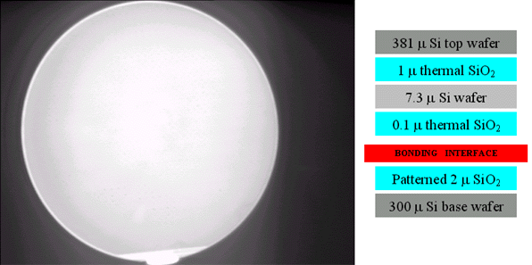
Figure 1. A micromachining technique based on SOI silicon wafers and wafer bonding. |
|
|
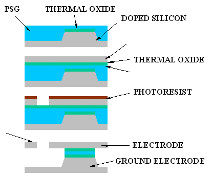
Figure 2. A process flow based on wafer bond of SOI wafer. |
|
|
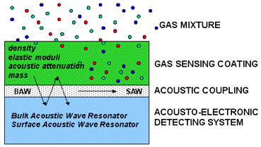
Figure 3. A basic structure of the acousto-electronic gas-sensing platform. |
Advanced sensors for detecting simultaneously various parameters such as temperature, pressure, radiation, gas and vapor concentration, odor, acceleration, inertia, electric and magnetic fields, and more must provide not only high signal-to-noise ratio in a wide dynamic range but also good cross-sensitivity. In general, the sensors consist of two elements: a detector and a platform that communicates with the detector through an active interface with variable electrical, mechanical, optical, or chemical impedance. The platform must be able to generate output electrical signals carrying the information provided by the detector.
Because today's silicon micromachining technology is highly sophisticated, MEMS employing silicon offer many advantages in the design of multifunctional sensors. Silicon, an ideal electronic material and also a high-performance mechanical material, can be micromachined by using chemical and electrochemical etch techniques. All classic technologies used in microelectronics manufacturing, including photolithography, diffusion, oxidation, ion implantation, and metal coating, can be applied in silicon micromachining. Techniques such as silicon-to-silicon and silicon-to-glass wafer bonding add strength to micromachining/microelectronics integration technologies, enabling development of new devices and multifunctional sensors. Wafer bonding and surface micromachining are two critical technologies competing in today's manufacturing of MEMS. Polycrystalline silicon-based surface micromachining, with its classic microelectronics technology, has been utilized more than wafer bonding. However, wafer bonding has a major advantage: it allows the use of single-crystal silicon instead of polycrystalline silicon. Single-crystal silicon improves the design of microacoustics and microoptics MEMS sensors because it has significantly lower acoustic losses and better optical properties than polycrystalline silicon. For example, at 500 MHz, single-crystal silicon has an attenuation coefficient of 3 dB/cm for longitudinal waves, which is comparable to the attenuation coefficient of crystalline quartz. Resonant structures can be readily micromachined using single-crystal silicon. A typical micromachining technique based on SOI silicon wafers and wafer bonding is shown in Figure 1. The process flow in Figure 2 is based on wafer bonding of SOI wafers and can be used to manufacture various integrated resonant devices and systems for adaptive optics. MEMS technologies offer the potential for complimentary multifunctional devices by integrating various systems and principles.
Bulk and Surface Acoustic Wave Sensors
The most common sensor platform is based on piezoelectric devices. Figure
3 shows the basic structure of the acousto-electronic gas-sensing platform.
Bulk and surface acoustic wave resonators have been used extensively in the
design of multifunctional physical and chemical sensors, including microbalances,1-3
viscosity sensors,4 humidity
sensors,5 immuno-detectors,6,7
gas sensors,8 ion-intercalation
monitors,9 and magnetic-
and electric-field sensors.10
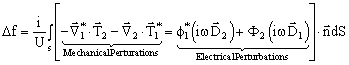
Because frequency may be measured with higher accuracy than any other parameter,
mechanical resonators are well suited for the design of high-sensitivity sensors.
Often, thin-film coatings sensitive to the measured parameter are deposited
on the resonator because changes in the physical or chemical parameters of the
film increase the resonance frequency shift. Resonator-based sensors measure
resonance-frequency shifts caused by mechanical, chemical, or electrical perturbations
of boundary conditions on the interface.3,11
Mechanical boundary conditions provide continuity of particle velocity and stress
on the interface boundary. A resonator without any load film in vacuum behaves
like an unbounded, stress-free plate. If the resonator is loaded with a thin
film, the boundary conditions will be modified. A dielectric film modifies mechanical
boundary conditions, while a conducting film modifies both mechanical and electrical
boundary conditions. A resonator coated with a film no longer has stress-free
boundaries. Mechanical and electrical perturbations cause resonant-frequency
shifts. With the assumptions of no internal electrical sources in quasistatic
approximation where ![]() and
and
![]() , where F
is the electric potential, and ho
is the electrical charge density, lossless boundaries and only external perturbations
the resonant frequency shift is given by:12
, where F
is the electric potential, and ho
is the electrical charge density, lossless boundaries and only external perturbations
the resonant frequency shift is given by:12
 |
|
|
and
|
|
|
|
and
|
|
|
|
 |
|
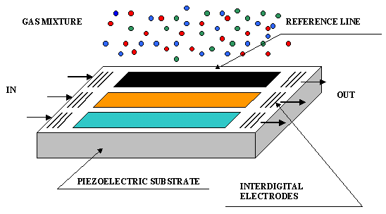
Figure 4. A surface acoustic wave platform using various sensing thin films deposited on the piezoelectric resonant line. |
|
|
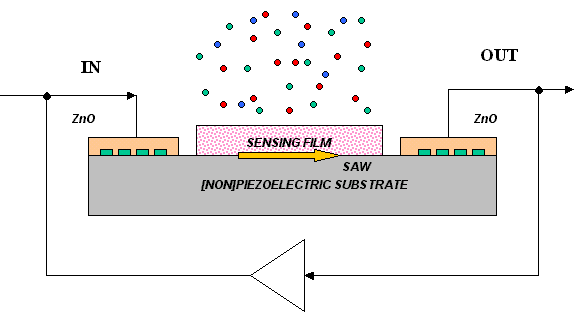
Figure 5. A SAW configuration using nonpiezoelectric substrate. |
Figure 4 shows a surface acoustic wave
platform using various sensing thin films deposited on the piezoelectric resonant
line. In general, acoustic shear wave modes that do not couple electrically
to a fluid are used to avoid heavy loss of acoustic energy and Q-factor degradation.
Shear horizontal (SH) plate modes (SH) and Love modes are most utilized for
surface acoustic wave devices. In a gas mixture, each film detects a corresponding
component. Figure 5 shows another surface
acoustical wave (SAW) configuration using silicon, a nonpiezoelectric substrate.
The interdigital transducers are coated with ZnO, a piezoelectric material that
might be deposited using reactive magnetron sputtering. The SAW line is part
of an oscillator circuit. When the sensing coating changes its mechanical parameters-which
happens in the presence of the gas to which partial pressure has to be measured-the
resonant frequency shifts because of changes in the SAW propagation velocity.
The reference SAW line, coated with passive glass film, is used for calibration.
Because of the small dimensions of a SAW line, numerous lines could be coated
with various sensitive films in order to detect a wide range of analytes. However,
various coatings provide various responses and often the response of a given
SAW-sensing element is heavily affected by cross-link interference.
To solve this problem, pattern recognition techniques have been used to analyze
the signals coming from chemical sensor arrays.13,14
Similar to natural biological sensors, pattern recognition techniques use databases
of previously measured and stored array responses to identify analytes detected
by SAW arrays. Pattern recognition techniques could help to identify a large
number of chemical species using a fixed set of sensors. The Q-factor of a free
resonator is very high. For bulk resonators, Q is of the order of 106
or higher, which allows the measurement of resonance-frequency shifts with accuracy
better than 0.01 Hz. Such accuracy is possible only if the oscillations of the
resonator are not suppressed. However, in many experiments, the quartz-crystal
resonator operates in harsh conditions, resulting in heavy damping of the oscillations.
Often quartz resonators are coated with thick material layers of unknown mechanical
properties or are immersed in high-viscosity liquids. In such cases, the damping
of the oscillations of the resonator results in a dramatic decrease of the Q-factor.
The resonance peak is wide, and the noise level is high. At resonant frequency,
the resonator has a maximum conductivity and behaves like a resistor, corresponding
to a zero-phase shift. The slope of the phase in the proximity of the zero phase
shift point is proportional to the Q factor (90� slope corresponds to Q �
�). A small frequency shift of the resonance peak may be measured with
high accuracy, which cannot be improved by the use of a second resonator as
a reference. The resonator, having a lower Q factor, decreases the accuracy
of the measurement of the difference between the resonance frequencies of the
two resonators.
Piezoelectricity and anisotropy of quartz change substantially the process of
acoustic mode generation. Only a few acoustic modes in quartz could be driven
piezoelectrically and the appearance of a multitude of overtones and new modes
in the resonance frequency band makes the selection of a particular mode extremely
difficult. In an isotropic medium, three independent acoustic modes with orthogonal
polarization (direction of particle motion) may propagate in any direction:
one longitudinal wave (the fastest wave in which polarization is parallel to
the wave vector) and two degenerate shear waves with the same velocity. In anisotropic
elastic solids, acoustic waves do not usually have particle motion polarized
either parallel or normal to the wave vector. One quasi-longitudinal and two
quasi-shear modes with different phase velocities and non-orthogonal polarizations
can propagate independently in each direction. In general, the phase and group
velocities are not collinear. Depending on the crystal symmetry, few crystallographic
directions could be defined as "pure-mode" directions. There are two classifications
of pure-mode directions: when the three propagating modes have orthogonal polarizations
(the polarization of the longitudinal mode coincides with the propagation direction)
and when phase and group velocities are collinear. In the case of a-quartz
(trigonal symmetry of group 32), the elements of symmetry are one 2-fold axis
(axis X) and one 3-fold axis (axis Z coinciding with the optical axis of quartz).
|
|
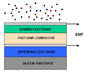
Figure 6. An electrochemical gas-sensing platform. |
AT-cut resonators are the most widely in frequency control because of their
high Q factor and low temperature coefficient. AT-cut resonators are favored
for acoustic sensor design. For an electrical field applied in the YZ plane,
two piezoelectric constants, e25
and e26, may be used to excite mechanical
vibrations. The plate's normal is in the YZ plane and the electric field may
be applied with the help of electrodes placed on the plate faces. The thickness-shear
mode (TS), with displacement along X and frequency given by the elastic modulus
c66, is dominant. However
the modes generated by the electric field applied to the resonator are coupled
through all types of elementary motion possible at the frequencies considered.
This complex polarization results in unpredictable sensor responses when the
resonator is in contact with another liquid or solid medium.
Electrochemical Sensors
Another family of multifunctional sensor systems is electrochemical gas sensors
(Figure 6), which use solid-state galvanic
cells to monitor partial pressures of gases such as CO2,
NOx, SOx,
and hydrocarbons in gas mixtures. The sensor operates as a battery: the electromotive
force (EMF) changes a function of chemical modifications of the cathode in the
presence of the gas according to the following arrangement:15
Pt electrode, gas | gas sensitive film |
ion conducto | reference electrode | Pt electrode
For example, to measure the EMF and the NO2 partial pressure, a galvanic cell of the following type can be used:
Pt | Na | Nasicon | NaNO3 | Pt, NO2, O2
The reaction in the cell is
Na + NO2 + 0.5 O2 = NaNO3
The relationship between the EMF and the NO2 partial pressure is given by:
EMF ≈ -DG[NaNO3] + DG[NO2] + kTIn P[NO2] + (kT/2)InP[O2]
Where G is the Gibbs energy, P is the partial pressure, k is the Boltzmann's constant, and T is absolute temperature.
|
|
|
|
 |
 |
|
|
|
|
|
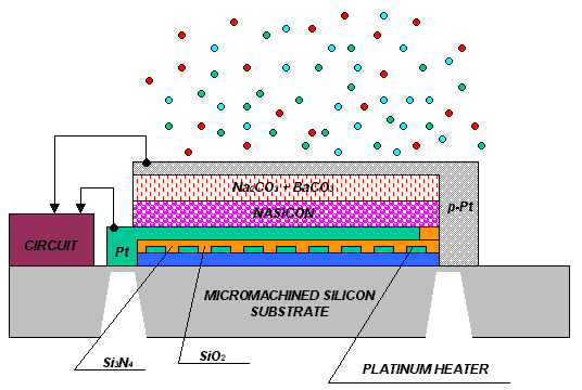
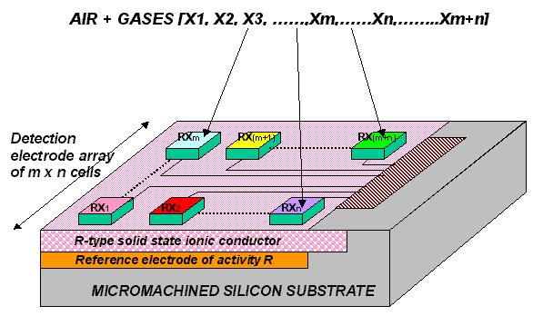
| Figure 7. An electrochemical CO2 gas sensor operating at 350�C. | Figure 8. A gas-sensor array fabricated using MEMS technology. | |
|
|
|
An electrochemical gas sensor for measuring partial pressure
of CO2 fabricated using thin-film technology
and silicon micromachining is shown in Figure
7. The sensor operates at 350�C and the whole structure is built on top
of micromachined silicon with platinum thin film heater. Thin Nasicon film is
the ion-conducting separator.16
The sensing electrode is a mixture of barium and sodium carbonate deposited
through reactive magnetron sputtering. The reference electrode is the isolation
film of silicon nitride covering the platinum heating elements. The micromachined
silicon substrate allows the heater to operate at 350�C while the surrounding
aria is at room temperature and the same silicon substrate could be used as
a base of the controlling electronics.
The fabrication technology of the sensor presented in Figure
7 allows integration of various gas sensors on the same substrate. Nasicon
is used for all sensors as an ion-conducting separator of the battery. Only
the sensing electrodes are different, as shown in Figure
8. For example, to detect NOx a sensing
electrode of sodium nitride can be used.17
1. C. Wei and
K. Rajeshwar, J.
Electrochem. Soc., 140 (1993), p. L128.
2. R. Oltra and I. O. Efimof,
J. Electrochem.
Soc., 141 (1994), p. 1838.
3. D. Ivanov and A. Yelon, J.
Electrochem. Soc., 143 (1996), p. 2835.
4. A. J. Ricco and S. L. Martin,
Appl.
Phys. Lett., 50 (1987), p. 1474.
5. G. Gerlach and K. Sager,
Sensors
and Actuator A, 43 (1994), p. 181.
6. M. Rapp et al., The 7th
Int. Conf. Sensors and Actuators (1997), p. 538.
7. J. Kondon, Y. Matsui, and
S. Shiokawa, The 7th Int. Conf. Sensors and Actuators (1997), p. 534.
8. J. Vetelino, R.K. Lade, and
R.S. Falconer, IEEE Trans. Ultrason., Ferroelect., and Freq. Contr.,
UFFC-34 (Piscataway, NJ: IEEE,
1987), p. 156.
9. K. Takeshita, W. Wernet,
and N. Oyama, J.
Electrochem. Soc., 141 (1994), p. 2004.
10. S.M. Hanna, IEEE Trans.
Ultrason., Ferroelect., and Freq. Contr., UFFC-34 (Piscataway, NJ: IEEE,
1987), p. 191.
11. D. Ivanov and A. Yelon,
Electrochem. Soc. Proceedings, 96-9 (1997), p. 110.
12. B.A. Auld, Acoustic
Fields and Waves in Solids, vol. II (New York: John
Wiley & Sons, 1973), p. 319.
13. X. Wang et al., Sensors
and Actuators B, 13 (1993), p. 455.
14. G.C. Osbourn et al., Solid-State
Sensor and Actuator Workshop (1994), p. 193.
15. W. Weppner, Mater.
Sci. Eng., B15 (1992), p. 48.
16. J.F. Currie et al.,
Ionic and Mixed Conducting Ceramics, vol. 94-12, ed. T.A. Ramananarayanan,
W.L. Worrell, and H.L. Tuller (Pennington, NJ: The
Electrochemical Society, 1994), p. 127.
17. N. Miura and S. Yao, Proc.
Int. Conf. Solid State Sensors and Actuators, "Transducer '91" (1991), p.
558.
Dentcho V. Ivanov is with the Microelectronics Research Center at the New Jersey Institute of Technology.
For more information, contact D.V. Ivanov, Microelectronics
Research Center, New Jersey Institute of Technology, 121 Summit St., R200, Newark,
New Jersey 07102.
Direct questions about this or any other JOM page to jom@tms.org.
| If you would like to comment on the October
2000 issue of JOM,
simply complete the JOM on-line critique form |
|||||
|---|---|---|---|---|---|
| Search | TMS Document Center | Subscriptions | Other Hypertext Articles | JOM | TMS OnLine |