|
|
|
|
http://www.tms.org/pubs/journals/JOM/0010/Rosenthal/Rosenthal-0010.html
|
|
|
|
|
|
http://www.tms.org/pubs/journals/JOM/0010/Rosenthal/Rosenthal-0010.html
|
|
|
TABLE OF CONTENTS |
|---|
|
|
The technique of Fourier transform infrared (FTIR) reflectometry has been advanced to characterize the thickness and optical properties of thin films commonly used in advanced integrated circuits (I.C.s). This article describes the demonstration of a new, high accuracy reflectometer to characterize the reflectance of ultrathin gate oxides and chemically amplified deep ultraviolet (UV) photoresist thin films. The gate oxide reflectance data were related to the deposition time to model the thermal oxidation growth kinetics. Model based analysis was employed to extract the dielectric function and thickness of the photoresist layers. Changes in the absorption features in the dielectric function were related to the exposure dose.
As the semiconductor industry moves to develop integrated
circuits (I.C.s) with smaller feature sizes, faster switching speeds, and lower
power consumption, the materials employed in the basic wiring, dielectric, and
photolithographic layers are changing dramatically. In particular, the paradigm
of aluminum/silicon dioxide interconnect technology, diffused, implanted, or
epitaxial active silicon layers, and mercury line photoresists (a paradigm that
has lasted for several decades with little change) is giving way to a new I.C.
architecture employing copper/low-k interconnects, silicon-germanium and silicon
on insulators based transistor structures, chemically amplified deep ultraviolet
(UV) and x-ray lithography, and new metal-silicide ohmic contact materials.
One unifying theme shared by these new materials is the greater complexity and
importance of composition in controlling their properties.
The goals of timely and cost effective integration of these new materials into
mainstream manufacturing has motivated the introduction of new metrology and
process control practices focused on meeting new specs on layer composition
as well as thickness. Furthermore, to meet the industry wide goals articulated
by National Technology Roadmap for Semiconductors (NTRS), the roles of both
old and new metrology are expected to shift from interactive off-line and stand-alone
measurement configurations to automated in-line and in situ configurations.
This shift is needed to enable overall increased automation of process control
tasks such as run-to-run control, fault detection and classification, as well
as to decrease the reliance on non-product wafers used for process control and
quality assurance. Ultimately, the goal is to employ non-destructive measurements
on every product wafer as a means to gather data to control the process.
Ultraviolet and visible (UV-VIS) reflectometry and ellipsometry has emerged
over the last decade as the most widely accepted method for production monitoring
of transparent thin films. Their excellent accuracy, sensitivity, and ability
to extract multiple parameters from a film stack have made them widely applicable
for many film processes. Nevertheless, UV-VIS techniques are insensitive to
compositional effects, and often suffer from complications associated with roughness
induced scattering, sample-to-sample variations in crystallinity and optical
properties, and correlations of parameters such as thickness and index of refraction
for the thinnest samples. In light of the increased interest in controlling
layer composition, in structures that often exhibit significant microroughness
and variations in microstructure, these issues are becoming increasingly important.
Infrared spectroscopy offers a metrology approach, complementary to UV-VIS techniques,
that provides excellent sensitivity to layer composition, including chemical
bond densities (through their vibrational mode intensities), and free carriers,
with enhanced immunity to roughness induced scattering. Because it can be implemented
as a reflectance sensor, infrared spectroscopy shares many of the inherent advantages
of UV-VIS spectroscopy as a non-destructive process control tool.
We have recently developed a new FTIR reflectometry tool optimized for the characterization
of films with complex chemistry. This new metrology tool employs two recent
inventions: a high sensitivity optical reflectometer design that can measure
thin films on transparent substrates while suppressing backside reflected light
that would otherwise interfere with the analysis of the front surface reflections;
and model-based fitting to extract the dielectric function of a layer from the
reflectance spectrum, thereby separating out the compositional information from
interference fringes and substrate related artifacts. The mid infrared dielectric
function, typically expressed in terms of the complex refractive index n +ik,
encodes a great deal of chemical information related to chemical bond related
vibrational modes, porosity, stress, and doping, in the form of free-carrier
absorption.
Samples of ultrathin thermal oxides and deep UV photoresist
were studied using the Fourier transform infrared (FTIR) system. Reflectance
spectra were acquired using a system incorporating the FTIR reflectometer equipped
with a linearized liquid nitrogen detector. Data were collected at an angle
of incidence of 47�, with an s polarization fraction of 0.43, in the spectral
range between 600 cm-1 and 5,000 cm-1. Reflectance data were referenced to lightly
doped silicon wafer samples. Overall, the instrument drift was observed to be
less than 1% over a 24-hour period, and with frequent references, reflectance
data were reproducible in the short term to better than 0.1%. As inputs to the
model-based analysis software, the angle of incidence and polarization of the
probing beam were carefully calibrated using samples of silicon and silicon
dioxide.
After the spectra were collected, model-based (curve fitting)
thin film algorithms were applied to analyze the data to determine layer thicknesses
and optical constants.1-5
The data of optical constants were then related to the layer composition or
process parameters. Employing a model for the film stack and the DF (optical
constants) of each of the layers in the film stack, the software performs a
transfer matrix calculation of the reflectance.6,7
The optimization or fitting algorithm then iteratively varies the model parameters
such as layer thicknesses, carrier concentrations, index of refraction, and
other dielectric function (DF) parameters, recomputing the simulated reflectance
until the weighted mean square difference is minimized between the measured
and simulated spectra.
The film stack model provides a parameterization of the structure that contains
a list of layers and compositions of the materials in each layer. The model
may include regions with abrupt and graded composition profiles. If present,
graded layers are approximated as segmented stacks of uniform layers, each slightly
different than its neighbors. The reflectance model computes a simulated reflectance
from the segmented layer stack model.
During fitting, the dielectric function models compute the frequency dependent
optical constants n and k from the layer compositions prescribed in the film
stack model. For particularly fast and accurate fitting with only a few free
parameters, constrained dielectric function models are tailored to the optical
behavior of the materials. For reflectance analysis, silicon, for example, is
nearly perfectly modeled in the infrared by a Drude term for the free carriers,
and a smooth weakly varying background dielectric function. While most dielectrics,
such as silicon dioxide, silicon nitride and photoresist have relatively simple,
compositionally insensitive Cauchy dielectric functions in the visible,8
in the infrared these materials generally exhibit significant chemical variability,
encoded in the vibrational absorption band structure. To analyze these compositionally
complex materials in the infrared, a more general approach is required to model
and extract dielectric functions of materials from reflectance spectra. In this
method, the dielectric function of the layer is modeled with a basis set of
damped harmonic oscillators, i.e. as a sum of Lorentzian terms (SOL), closely
spaced in frequency, with equal damping constants and spacing. The arrays of
oscillators are located in the spectral regions, where absorption is expected
in the film. The width and spacing of the Lorentzians set describing these oscillators
are fixed at values that depend on the desired spectral resolution. During the
fit, the amplitudes of the oscillators, high frequency dielectric constant,
and layer thickness are varied to fit the model to the measured data. This procedure
provides a robust, well-conditioned extraction of a dielectric function of a
layer, independent of the layer thickness, using only the reflectance spectrum.
By virtue of the properties of the Lorentzian oscillator basis set, the solutions
are implicitly Kramers-Kronig consistent, and can model a DF of arbitrary shape
or complexity. This combination of powerful algorithms and accurate reflectometry
data provides the basis for analyzing a wide variety of thin film materials.
 |
 |
 |
||
|
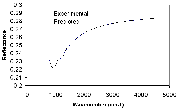
Figure 1. Measured and fitted reflectance of 4.9 nm oxide film. |
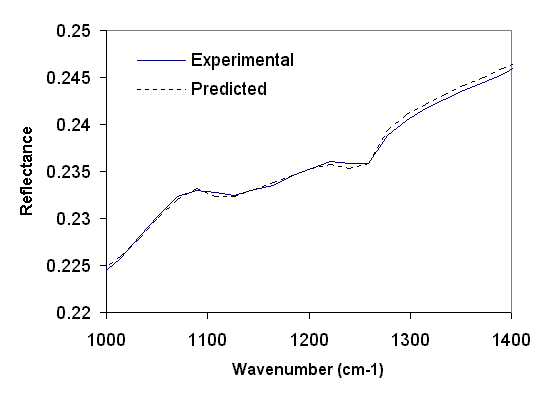
Figure 2. Magnified view of the Si-O stretch spectral region. |
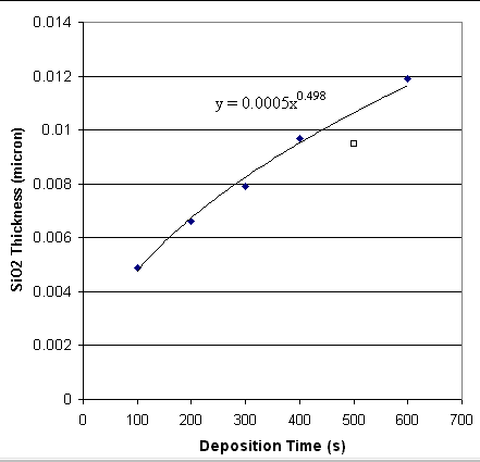
Figure 3. SiO2 thickness measured by FTIR for a series of ultrathin thermal oxides on heavily doped substrates as a function of deposition time, overlaid with a power-law fit. The open square symbol is a suspected misprocessed wafer. |
||
|
|
|
|
A series of gate oxide films were acquired from the New Jersey Institute of
Technology (NJIT). The films were fabricated in a rapid thermal processor with
deposition times of 100, 200, 300, 400, 500, and 600 seconds; all processed
at the same temperature. The substrates were heavily doped p+ silicon. Figure
1 shows the measured and fitted reflectance of the 100-second sample. The
spectra were fit to a multiparameter model in which the substrate carrier concentration
and scattering rate, as well as the oxide thickness, were allowed to vary during
the analysis. Literature values for the oxide DF were employed for these fits.9
The oxide layer thickness was encoded mostly in the optical vibrational modes
in the band around 1,100 wavenumbers, while the substrate carrier concentration
affected the spectrum broadly, with a dramatic plasma edge visible around 700
wavenumbers. Figure 1 shows that the
fitted spectrum is virtually identical to the measured data. The fits were similarly
excellent for all the wafers, indicating that the films were high quality oxide
layers, and that the analysis model employed an accurate description of the
optical properties of both the substrate and film.
Figure 2 shows an expanded view of the absorption region of the spectrum around 1,000-1,300 wavenumbers. The SiO2 film has a transverse vibrational mode at 1,070 wavenumbers whose amplitude is indicative of the surface density of silicon-oxygen bonds. An associated longitudinal mode is also visible at 1,250 wavenumbers. The longitudinal mode position is much more dependent on film stress and density than the transverse mode and can be considered an indicator of film quality. Figure 2 shows that the measured LO mode is shifted to slightly higher frequency than that observed in the fitted reflectance, which was calculated using bulk thermal oxide optical constants. This indicates the possible presence of stress in the film perturbing the index of refraction.
|
Wafer #
|
Deposition Time(s)
|
SiO2
Thickness (mm)
|
|
|
|
|
|
1
|
100
|
0.0049
|
|
2
|
200
|
0.0066
|
|
3
|
300
|
0.0079
|
|
4
|
400
|
0.0097
|
|
5
|
500
|
0.0095
|
|
6
|
600
|
0.0119
|
|
|
||
The extracted SiO2 layer thicknesses, summarized
in Table I, ranged from approximately 5 nm to 12 nm. A
repeatibility study on several of the samples established the precision (1 sigma)
of the measurement to be around 0.7 �. The SiO2
thickness vs. deposition time is plotted in Figure
3, along with a fit to a power law. This fit resulted in an exponent of
0.498, a nearly perfect square root law. This square root dependence on time
is commonly observed in diffusion limited processes such as thermal oxidation.
All but wafer #5 fell within 0.2 nm of the trend line. This sample, labeled
as a 500-second growth, was nearly identical to the 400-second sample.
|
|
|
 |
 |
|
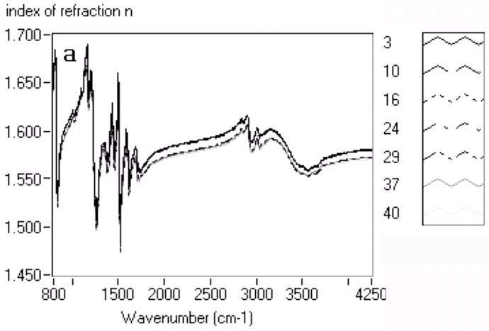
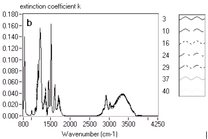
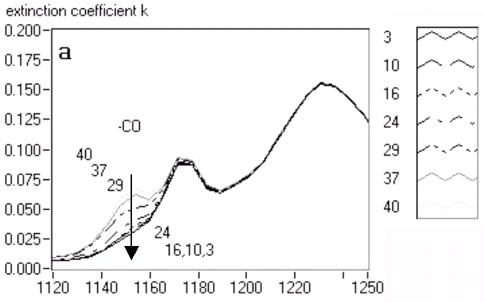
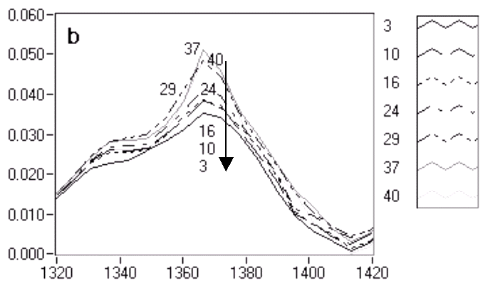
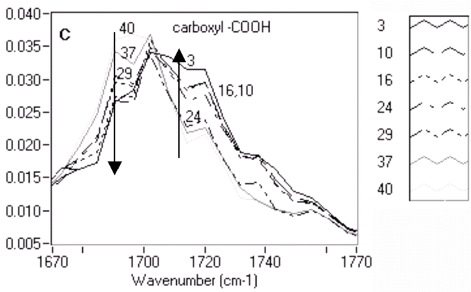
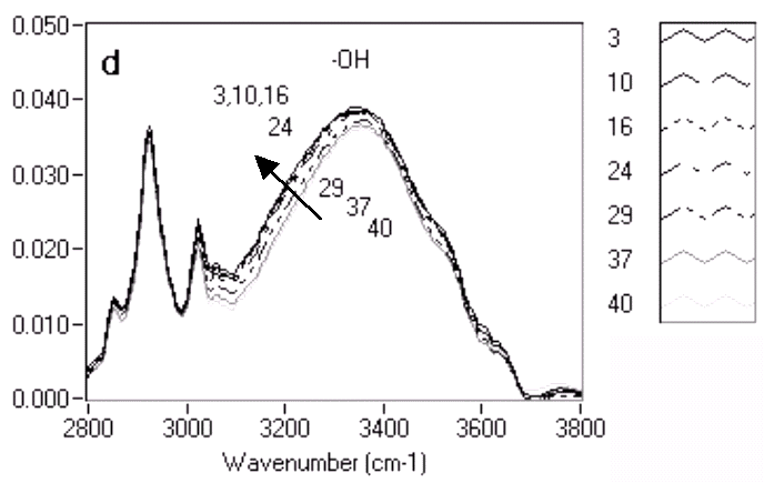
Figure 4. Extracted index of refraction and extinction coefficient for the UV5 resist as a function of exposure level. |
|
|
|
|
A chemically amplified Deep UV (DUV) photoresist sample was analyzed to explore
the ability to characterize an organic thin film with extremely complicated
photochemistry and optical constants. A wafer was obtained from National Semiconductor
with a layer of Shipley UV5 photoresist deposited, exposed and post-baked according
to the manufacturer's recommendations. A series of 1-cm fields on the wafer
was exposed with different doses to investigate the effect of exposure dose
on the infrared properties of the resist. Each of the fields was measured using
the infrared reflectometer, and analyzed for the resist dielectric function
using the SOL based dielectric function extraction algorithm. The DF data in
Figure 4a, Figure
4b, Figure 5a, Figure
5b, Figure 5c, and Figure
5d are labeled with increasing label numbers for decreasing doses. Figure
4a and Figure 4b show the extracted
index of refraction and extinction coefficient, while Figure
5a, Figure 5b, Figure
5c, and Figure 5d show the expanded
spectral regions that exhibited the most dramatic chemistry-related changes.
The figures show clear systematic variations with exposure dose, both in the
detailed absorption bands as well as in the high frequency index of refraction.
The reduction of the band around 1,150 cm-1
corresponds to -CO groups reacting and producing -OH groups, for which a corresponding
increase is observed in the 3,100-3,500 cm-1
region. Changes in the 1,700 cm-1 region have
been attributed to the deprotection reaction involving ester bonds reacting
with the photo-generated acid to yield carboxylic acids.10
|
|
|
 |
 |
 |
 |
|
|
|
| Figure 5. Variations in chemistry for UV5 resist. | |
|
|
|
By combining model-based infrared spectral analysis with high performance reflectometry hardware , it is possible to extract quantitative data on multiple parameters related to film properties. The technique has a unique sensitivity to film composition, which is broadly applicable to a wide range of films including ultrathin oxides, doped semiconductors, and complex materials such as photoresists and low-k dielectrics. With wider application, FTIR could significantly enhance the development, introduction, and production of the new materials currently being considered for future generations of high performance I.C.s. More work is clearly needed to develop a deeper understanding of the relationship between the infrared optical properties of thin films and their process and performance parameters.
The authors gratefully acknowledge the support of the NSF SBIR grant No. DMI-9631216 and No. DMI-9860798, and Army SBIR Grant No. DAAH04-C-0090 for the generous support for the R&D programs that generated these results.
1. S. Charpenay
et al. "Model-based Analysis for Precise and Accurate Epitaxial Silicon Measurements,"
Solid, State
Technology (July 1998).
2. B.W. Fowler et al., "The
Measurement of Sub-micron Epitaxial Layer Thickness and Free Carrier Concentration
by Infrared Reflectance Spectroscopy," Proc. Electro-Chemical Soc., 94-33
(1994), p. 254.
3. S. Liu et al., "FT-IR Spectroscopy
as a Process Monitor for Integrated Circuit Manufacturing," SPIE
(January 1993).
4. Peter A. Rosenthal, "Integrated
FTIR Reflectometer Controls Semiconductor Fabrication Process," Laser Focus
World-Design and Applications, 34 (April 1998), pp. 173-176.
5. T. Buffeteau and B. Desbat,
Applied
Spectroscopy, 43 (6) (1989), pp. 1027-1032.
6. F. Abeles, Advanced Optical
Techniques (Amsterdam: North-Holland, 1967).
7. K. Yamaoto and H. Ishida,
Applied
Spectroscopy, 48 (7) (1994), p. 775.
8. E. Hecht and A. Zajac, Optics,
2nd ed. (Reading, MA: Addison-Wesley
Publishing Co., 1987).
9. E. Palik, Handbook of
Optical Constants of Solids (New York: Academic
Press, Inc., 1985).
10. N. Jakatdar et al., "Novel
Metrology for the DUV Photolithographic Sequence," Characterization and Metrology
for ULSI Technology, Seiler et al. (College Park, MD: The
American Institute of Physics, 1998).
P.A. Rosenthal, J. Xu, and S. Charpenay are with On-Line Technologies, Inc.; J.E. Cosgrove is with Advanced Fuel Research, Inc.; and N.M. Ravindra is with the New Jersey Institute of Technology.
For more information, contact Peter Rosenthal, On-Line Technologies,
Inc., 87 Church Street, East Hartford, Connecticut 06108; (860) 291-0719; fax
(860) 289-7975, e-mail prosenth@online-FTIR.com
or e-mail N.M. Ravindra at nmravindra@home.com.
Direct questions about this or any other JOM page to jom@tms.org.
| If you would like to comment on the October
2000 issue of JOM,
simply complete the JOM on-line critique form |
|||||
|---|---|---|---|---|---|
| Search | TMS Document Center | Subscriptions | Other Hypertext Articles | JOM | TMS OnLine |