 |
53 (6) (2001), pp. 28-32. |
|---|
Lead-Free Solder: Research Summary
|
53 (6) (2001), pp. 28-32. |
|---|
|
TABLE OF CONTENTS |
|---|
|
|
 |
|
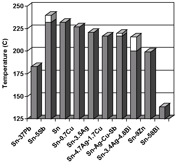
Figure 1. Chart of lead-free solder tem-peratures (dark–solidus; light–liquidus). |
A variety of lead-free solder alloys were studied for use as flip-chip interconnects including Sn-3.5Ag, Sn-0.7Cu, Sn-3.8Ag-0.7Cu, and eutectic Sn-37Pb as a baseline. The reaction behavior and reliability of these solders were determined in a flip-chip configuration using a variety of under-bump metallurgies (TiW/Cu, electrolytic nickel, and electroless Ni-P/Au). The solder microstructure and intermetallic reaction products and kinetics were determined. The Sn-0.7Cu solder has a large grain structure and the Sn-3.5Ag and Sn-3.8Ag-0.7Cu have a fine lamellar two-phase structure of tin and Ag3Sn. The intermetallic compounds were similar for all the lead-free alloys. On Ni, Ni3Sn4 formed and on copper, Cu6Sn5 Cu3Sn formed. During reflow, the intermetallic growth rate was faster for the lead-free alloys, compared to eutectic tin-lead. In solid-state aging, however, the interfacial intermetallic compounds grew faster with the tin-lead solder than for the lead-free alloys. The reliability tests performed included shear strength and thermomechanical fatigue. The lower strength Sn-0.7Cu alloy also had the best thermomechanical fatigue behavior. Failures occurred near the solder/intermetallic interface for all the alloys except Sn-0.7Cu, which deformed by grain sliding and failed in the center of the joint. Based on this study, the optimal solder alloy for flip-chip applications is identified as eutectic Sn-0.7Cu.
Metallic lead combined with tin forms a low melting-temperature
alloy that is extensively used for electronic interconnects. However, medical
studies have shown that lead is a heavy-metal toxin that can damage the kidneys,
liver, blood, and central nervous system. Less than one percent per year of
the global lead consumption is used in solder alloys for electronic products
but electronics and electrical systems make up an increasingly larger fraction
of landfills.1 The issue
of lead leaching from landfills into the water table has raised alarms as a
potential source of long-term contamination of soil and ground water. International
laws have recently been proposed to limit or ban the use of lead in manufactured
products. The most aggressive and well-known effort is the European Union’s
Waste in Electrical and Electronic Equipment directive that proposes a ban on
lead in electronics by 2008. The Japanese Environmental Agency has proposed
that lead-containing scrap must be disposed of in sealed landfills to prevent
lead leaching. The Japanese
Ministry of International Trade and Industry and the Japan Automobile Industries
Association called for a 50% reduction of lead in vehicles (excluding batteries)
by 2001 and a 33.3% reduction by 2003.2
Electronic-equipment manufacturers have responded to these proposed bans in
a variety of ways. Many companies have not taken a stance hoping that legislation
will not be enacted. Other companies have aggressively pursued solutions to
the proposed bans and are using lead-free products as a “green” marketing strategy.
Motorola, as a corporation,
has introduced Environmentally Preferred Products and, in 2001, will release
new lead-free products.
Extensive research on lead-free solders has been published over the past decade.
A comprehensive review of lead-free solders was performed by Glazer,3,4
and, since that time, research has focused on carrier-to-board (surface-mount
and through-hole) interconnects.5–15
A growing area of interest is in lead-free solders for flip-chip interconnects.
Flip-chip interconnects are the electrical and mechanical connections between
the semiconductor integrated circuit and the package (or board for direct-chip
attach). These interconnects are formed on the periphery or in an area array
on the top surface of an active die. An under bump metallurgy (UBM) forms the
solderable surface on the die. The UBM also acts as a diffusion barrier between
the tin and the solder and must be thick enough to withstand interactions (intermetallic
formation) between the solder and UBM. Flip-chip interconnects are smaller (on
the order of 100 mm diameter) than surface-mount
joints and are projected to have pitches that shrink below 150 mm.
Flip-chip interconnects must be able to withstand a potentially high level of
strain mismatch between tin and an organic substrate. Flip-chip technology has
moved from ceramic packaging with high lead solder (97.5Lead-2.5Sn) to an organic
package that requires lower temperature reflow (<260ºC). This can be accomplished
by bumping the die with high lead solder then joining it to an organic board
with eutectic tin-lead, but this method adds costs and can be eliminated with
a monolithic solder. The joints must withstand board-level reflow environments
compatible with joining to organic substrates that, again, have a maximum reflow
temperature of 260ºC. The lead-free solder must meet these requirements and
perform at, or above, the level of performance of the eutectic tin-lead solder
it is intended to replace.
One additional benefit of a lead-free flip-chip interconnect is the reduction
of pb210 -created alpha-particle radiation.
Due to their proximity to active elements, the flip-chip solder interconnects
should have minimal levels of alpha-particle radiation to limit soft errors
in complementary metal-oxide semiconductor (CMOS) technology that become more
critical as cell size on the die is reduced.16,17
The elemental constituents of lead-free solders (tin, copper, silver, bismuth,
indium, and antimony) do not radioactively decompose, so alpha-particle radiation
is minimal.
Lead-free solders for electronic applications are based on
tin-rich compounds that fall into a melting temperature range similar to the
traditional eutectic lead-tin solder alloys (183ºC). These include eutectic
Sn-3.5Ag with alloying elements of bismuth, copper, antimony, indium, or zinc.
Other alloys based on the tin-copper, tin-indium, tin-antimony, tin-bismuth,
and tin-zinc systems have also been proposed. A small two-phase region (temperature
difference between liquidus and solidus) is desired because it prevents the
joint from moving and becoming disturbed during solidification. Binary or ternary
near-eutectic alloys are also desired because simpler alloys reduce the potential
for compositional variations that affect the behavior of the solder joint. A
chart of the melting temperatures of potential solder alloys is shown in Figure
1. The alloys Sn-0.7Cu, Sn-3.5Ag, and Sn-3.8Ag-0.7Cu were immediately eliminated
as promising flip-chip solder alloys based on the selection criteria. Eutectic
Sn-37Pb was included as a control. The tin-antimony alloy was deemed to have
too large a two-phase region and the liquidus temperature of 240ºC was
too high for chip attachment to organic substrates (a process temperature of
245ºC is desired). The tin-zinc alloy had too many processing difficulties
due to the rapid oxidation behavior of the zinc in the molten state and corrosion
susceptibility of the alloy after solidification. The tin-silver-bismuth alloy
had too large a two-phase region. The Sn-Ag-Cu-Sb was not studied because it
was feared that in a flip-chip application the solder would damage the die rather
than deform due to the high strength of the alloy.18
Flip-chip interconnects are part of a package that must undergo carrier-to-
board reflow that occurs, at a minimum, at 220ºC. The tin-bismuth eutectic
alloy melts at far too low a temperature (138ºC) to withstand this reflow.
The alloys can be processed on silicon die either as solder paste stencil printed
on the defined UBM pads or through direct plating on the UBMs.
The UBMs used in this study were selected based on prior experience with these
structures with eutectic tin-lead alloys. The UBMs were sputtered TiW/plated
copper, electroless plated Ni-P/immersion gold, and electrolytic nickel (used
only for solder plating). The nickel was chosen because it reacts slowly, compared
to copper or gold, with tin-rich solders. The TiW/Cu used sufficient copper
to survive multiple reflows with the tin-rich alloys.
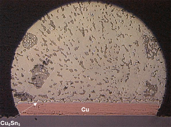
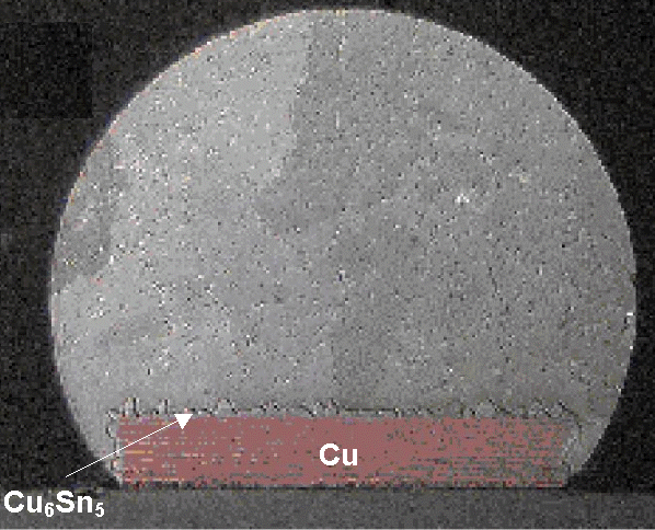
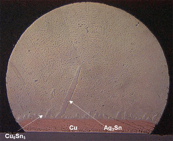
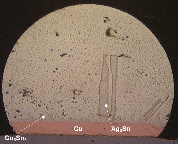
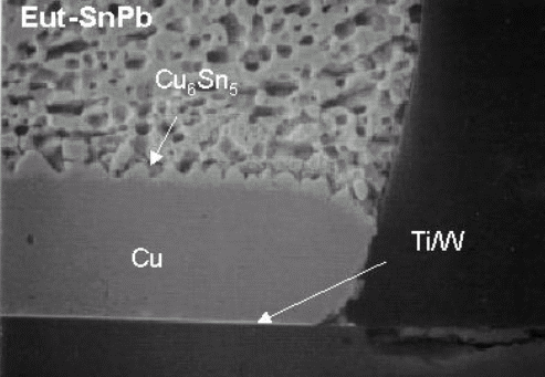
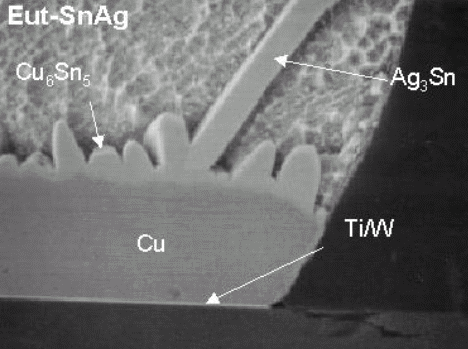
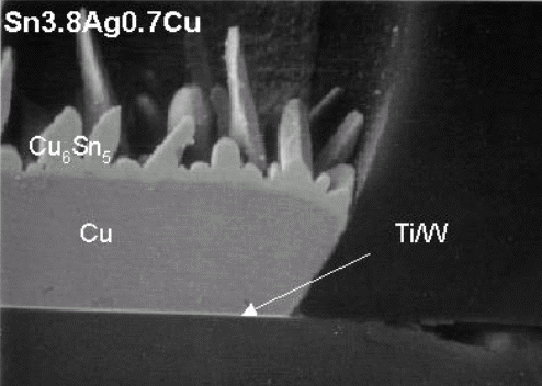
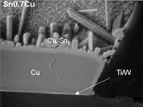
The microstructure of the solder alloys studied are shown in Figure 2, Figure 3, Figure 4, and Figure 5. The tin-lead eutectic has a structure of tin-rich and lead-rich phases that form as lamella (Figure 2). Similarly oriented lamella form cells, or colonies, separated by slightly coarsened cell boundaries. This structure is susceptible to heterogeneous microstructural evolution that concentrates strain at the cell boundaries and causes them to further coarsen and, eventually, be the site of failure. In the fine scale of the flip-chip interconnect, only a few cells are present in each bump but heterogeneous coarsening and failures are still observed.19
|
|
|
|
 |
 |
|
|
Figure 2. An optical micrograph of the microstructure of Sn-37Pb solder in a flip-chip bump on a copper UBM. |
Figure 3. An optical micrograph of the microstructure of Sn-0.7Cu solder in a flip-chip bump on a copper UBM. |
|
|
|
|
|
 |
 |
|
|
Figure 4. An optical micrograph of the microstructure of Sn-3.5Ag solder in a flip-chip bump on a copper UBM. |
Figure 5. An optical micrograph of the microstructure of Sn-3.8Ag-0.3Cu solder in a flip-chip bump on a copper UBM. |
|
|
|
|
Figure 3 shows the Sn-0.7Cu microstructure.
This solder is composed of large, tin-rich grains with a fine dispersion of
Cu6Sn5 intermetallics.
The solder grains, which form and grow out from the bond pad interfaces, are
large, on the order of 20–50 mm.
The Sn-3.5Ag microstructure consists of a fine structure of alternating tin-rich/Ag
3 Sn intermetallic lamella (Figure 4).
Grain colonies also form in this microstructure but the boundaries are not coarsened.
In addition to the fine Ag3Sn intermetallics,
large needles of Ag3Sn are present and are
typically attached to one of the bump-pad interfaces.
The Sn-3.8Ag-0.7Cu alloy has a structure of tin-rich grains with Ag3Sn
and Cu6Sn5
intermetallics dispersed throughout (Figure
5). The Ag3Sn also forms as large plates
attached to the interfacial intermetallics.
When the molten solders come into contact with the nickel or copper surfaces,
they wet and react to form interfacial intermetallics. The intermetallics grow
out into the solder as rods, or plates, and continue to grow when the solder
is solid. Even though all the solders studied are tin-rich, the morphology and
reaction kinetics differ between alloys.
On copper, Sn-37Pb forms a two-phase intermetallic of Cu6Sn5
adjacent to the solder and Cu3Sn adjacent
to the copper. The Cu3Sn is planar with a
columnar grain structure and the Cu6Sn5
consists of elongated nodules. On nickel, eutectic tin-lead forms irregularly
shaped Ni3Sn4.
The formation and growth of the interfacial intermetallics between copper, nickel,
and eutectic tin-lead solder are well known.18–20
The intermetallics follow parabolic growth kinetics and do not extensively spall
off into the solder.
|
|
||||
 |
 |
 |
||
|
Figure 6. SEM micrographs of the lead-free solders on an electroless nickel UBM showing the morphology of the interfacial intermetallics. |
||||
|
|
||||
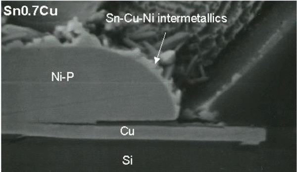
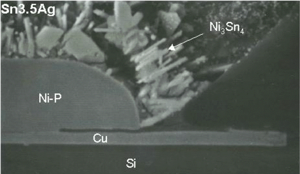
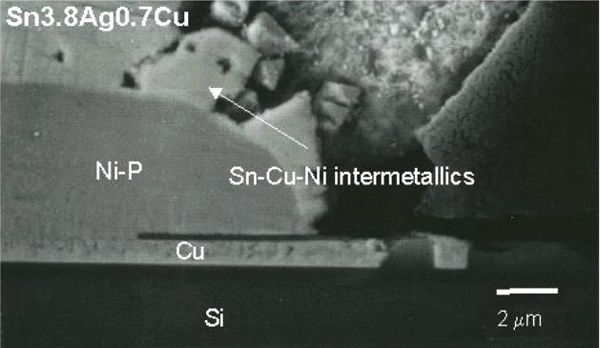
The intermetallic formation for the lead-free solders on nickel after two
reflows is shown in Figures 6a, 6b,
and 6c. Two reflows represent typical
processing for flip-chip interconnects. The first reflow represents ball formation
on the wafer, while the second represents flip-chip to substrate interconnect.
Figures 6a, 6b,
and 6c show the structure of the interface
on electroless nickel-phosphorus, but the same observations were made for the
electrolytic nickel UBM. The intermetallic that forms is Ni3Sn4.
The Ni3Sn4
intermetallic between Sn-0.7Cu and nickel is thin, regular, and is the most
uniform of the lead-free alloys. For Sn-3.8Ag-0.7Cu, the intermetallic is thicker
but has the same regular chunky morphology as for Sn-0.7Cu. TheSn-3.5Ag solder
on nickel has a different intermetallic morphology that consists of nodules
and chunks of Ni3Sn4
that spall off into the solder. This morphology has been attributed to the lack
of copper in the solder. It is hypothesized that the copper acts to saturate
the solder with respect to the nickel and inhibits dissolution and spalling
of the intermetallic into the solder.21
However, this mechanism remains to be fully understood.
The growth of interfacial intermetallics while the solder is in the solid-state
is of concern for flip-chip interconnects. If the intermetallic layer coarsens
significantly, it can consume the UBM and cause the joint to dewet at the layer
beneath the UBM. Also, because the intermetallic is brittle, if it becomes a
significant fraction of the solder joint, it can act as a site for crack initiation
and propagation when the joint is deformed.
|
|
 |
|
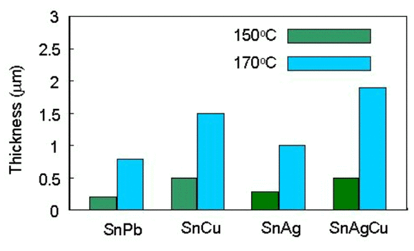
Figure 7. Thickness of consumed copper for the solders on electroless Ni-P/Au UBM. |
|
|
The consumption of the nickel layer by the formation of Ni3Sn4
intermetallic during solid-state aging for each of the solder studied is shown
in Figure 7. The solders were aged for
1,000 hours at 150ºC and 170ºC. Figure
7 shows results on an electroless Ni-P/Au UBM (similar results were observed
on the electrolytic nickel UBM). For all solders studied, less than 2 mm of
nickel was consumed while transforming into Ni3Sn4.
Because the nickel reacts slowly with tin-based solders, it is preferred for
tin-rich UBM structures. The lead-free solders consume more nickel and form
more slightly more intermetallic than tin-lead eutectic solder. but this increase
is relatively small. The Ag3Sn intermetallic
plates are attached to the Ni3Sn4
interfacial intermetallics, similar to that observed on the copper UBM (Figure
4 and Figure 5).
Figures 8a, 8b,
8c, and 8d
show SEM micrographs of the solders on a copper UBM after two reflows. The intermetallic
that forms is Cu6Sn5
, no Cu3Sn was found but it may have been
too thin to be observed. The interfacial intermetallic has the same morphology
for all the lead-free alloys as for tin-lead eutectic.The intermetallic consists
of regularly spaced nodules of Cu6Sn5.The
silver-containing solders all have large Ag3Sn
intermetallics that are attached to the Cu6Sn5
interface (Figure 4 and Figure
5). All three lead-free alloys also have small, discrete particles of Cu6Sn5
present in the bulk of the solder. For Sn-0.7Cu and Sn-3.8Ag-0.7Cu, the copper
is present in the solder before joining to the UBM. For the Sn-3.5Ag solder
theCu6Sn5
is present due to the dissolution of some of the UBM into the solder. Spalling
of the interfacial intermetallics into the molten solder was not observed, probably
due to the presence of copper in each of the solders during reflow. The copper
inhibits growth and spalling of the intermetallic because it saturates the solder.22
Of the three lead-free alloys on copper, theSn-0.7Cu solder structure is the
most uniform, and has the thinnest intermetallic structure.
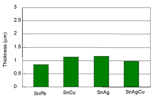
One of the concerns of using tin-rich, lead-free solders is the reaction of
the copper with the solders is feared to be so fast that the UBM will dissolve
during reflow. A plot of the copper consumed after two reflows for tin-lead
and the lead-free solders is shown in Figure
9. The lead-free solders consume only 10–20% more copper than tin-lead,
which is less than 2 mm after 2 reflows. A plot of
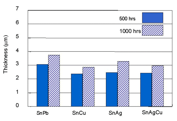
copper consumed during solid-state aging is shown in Figure10
for the solders on copper at 150ºC for 500 and 1,000 hours. In the solid
state, the copper was consume data slower rate in lead-free solders than for
eutectictin-lead. The lead appears to play a role in enhancing intermetallic
growth, perhaps by enhancing tin diffusion to the intermetallic/solder interface.Of
the alloys studied, Sn-0.7 Cu had the slowest consumption rate of the copper
UBM.
|
|
|
|
 |
 |
|
 |
 |
|
|
Figure 8. SEM micrographs of the lead-free solders on a copper UBM. |
||
|
|
||
|
Alloy
|
A (s–1)
|
a
|
n
|
Q (kJ/mol)
|
Ref.
|
|
|
|
|
|
|
|
|
Sn-40Pb
|
2.48 ´
104
|
0.0793
|
3.04
|
56.9
|
|
|
Sn-40Pb
|
1.1 ´
10–12
|
6.3
|
20
|
||
|
Sn-3.5Ag
|
9.3 ´
10–5
|
6.05
|
61.2
|
||
|
Sn-3.8Ag-0.7Cu
|
2.6 ´
10–5
|
3.69
|
36
|
||
|
Sn-1Cu
|
1.41 ´
10–8
|
8.1
|
79.4
|
||
|
|
|||||
The flip-chip solder joint must mechanically hold the chip to asubstrate, but
the solder can not impose significant strain to the semiconductor device or
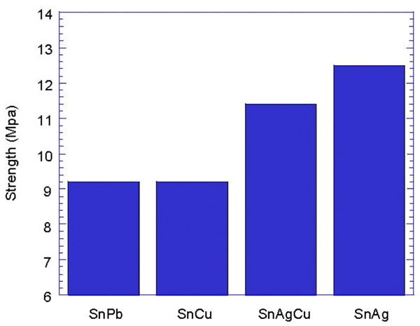
the device could crack and fail. The shear strength of the solder alloys is
shown in Figure11. The strength of the
solder alloys is a measure of the ability of the flip-chip interconnect to be
compliant to the imposition of strain. Sn-37Pb and Sn-0.7Cu solder bumps have
similar values of shear strength while the Sn-3.8Ag-0.7Cu is 20%stronger.TheSn-3.5Ag
solder alloy has the greatest shear strength at 25% greater than Sn-0.7Cu.The
shear failure for all joints tested occurred solely through the solder. The
solder joint strength and failure mode were similar to, and independent of,
the UBM type. Eutectic Sn-3.5Ag, and the companion Sn-Ag-X alloys (including
tin-silver-copper), have shown susceptibility to brittle interfacial delamination
in tensile 18 and shear
tests 23 for surface
mount interconnects. The failure occurs at the intermetallic/solder interface
where one side of the fracture shows intermetallic and the other side reveals
an impression of where the intermetallic grew in to the solder. It is not clear
why the Sn-Ag(-X) solder/intermetallic interface is so weak. There is some evidence
18 that silver segregates
to the interface and weakens it by “poisoning.” The brittle fracture is exacerbated
with gold contamination.24
Creep behavior is important for flip-chip interconnects because the solders
deform to relax stress over time when held at a constant strain.The creep rate
of a solder must be sufficiently fast so that the strain is minimized in joined
bulk components.However, the creep rate must not be so fast that the components
move over time. The creep behavior of solders can be summarized empirically
using one of two equations:
| Dg/dt = Asn e–Q/RT | (1a) |
| Dg/dt = Asinh(as)n e–Q/RT | (1b) |
where dg/dt is the creep rate in shear, A is a constant, a is the stress constant, s is the flow stress, n is the stress exponent, and Q is the creep activation energy. Equation 1a works well for creep mechanisms that remain constant over all test temperature. Equation 1b is the Garofalo, or sinh, creep relation that captures up to two different creep mechanisms in a single formulation. Creep tests were not performed in this study but have been investigated to some extent in the published literature.25-28 Table I represents the fitted results of creep tests on lead-free solders using these equations.Results are presented for tin-lead using Equation 1a and Equation 1b but the Garofalo fit was much better.29 The creep rate of high tin-content solders is slower than tin-lead.
|
|
|
|
||
 |
 |
 |
||
|
Figure 9. Consumed copper thickness after two reflows for the solders on a copper UBM. |
Figure 10. Bar chart of the consumed copper thickness of the solders on a copper UBM after aging for 500 hours and 1,000 hours at 150 C. |
Figure 11. Shear strength of the solder flip-chip bumps. |
||
|
|
|
|
|
|
 |
|
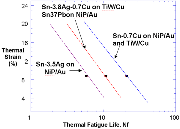
Figure 12. Plot of thermal fatigue life as a function of applied thermal strain for the Sn- 3.5Ag, Sn-37Pb, Sn-3.8Ag-0.7Cu, and Sn- 0.7Cu. |
|
|
Eutectic Sn-3.5Ag has greater strength and a higher creep resistance than eutectic
tin-lead.29 The creep
behavior of Sn-3.8Ag-0.7Cu is similar to Sn-3.5Ag and has been found to have
the highest creep resistance of the lead-free alloys.30
The steady-state creep behavior for tin-copper has been found to be faster than
eutectic tin-lead.The faster creep rate of tin-copper is desired for flip-chip
applications because damage can be accommodated by the solder, rather than the
more brittle joined components. Furthermore, a faster creep rate often translates
into a longer thermomechanical fatigue lifetime.
Temperature variations encountered during use conditions, combined with the
materials of differing coefficients of thermal expansion in the electronic package,
result in cyclic temperature and strain on the solder joints. Glazer presented
a summary of work on lead-free solders through 1994 and concluded that the thermomechanical
fatigue data for low melting-point solders are scarce and appear contradictory.3,4
The published data has primarily focused on surface mount interconnects; thermomechanical
fatigue data in a flip-chip configuration is still needed.
A diagram of thermal fatigue life vs. strain range was obtained, as shown in
Figure 12, using the characteristic
life extracted from Weibull plots of the thermomechanical fatigue data and thermal
strain range calculated from Equation A both for the
0ºC–100ºC and–40ºC–125ºC tests. This data was collected
on flip-chip packages with no underfill. By eliminating the underfill, this
study evaluated the relative thermal fatigue performance of different lead-free
solders and characterized the failure mechanisms. Although the strain evaluated
here tends to be much higher than that of packages with underfill encapsulation,
the failure mode remains valid. The thermal fatigue failure data follows a power
law function. In Figure 12, the thermal
fatigue data from Sn-0.7Cu flip-chip joints on both NiP and TiW/Cu UBMs fall
onto the same straight line. The thermal fatigue performance of Sn-0.7Cu is
UBM independent and is confirmed by the failure analysis discussed below, where
failures occurred solely through the solder joint. The cross sections of the
failed joints shown in Figures 13a,
13b, 13c,
and 13d are on the TiW/Cu UBM, but
similar failure behavior was exhibited for the electrolytic nickel and electroless
nickel/gold UBM structures. Sn-3.8Ag-0.7Cu and eutectic tin-lead have a similar
thermomechanical fatigue life. Sn-3.5Ag has the shortest thermal fatigue lifetime.
|
|
|
|
 |
 |
|
 |
 |
|
|
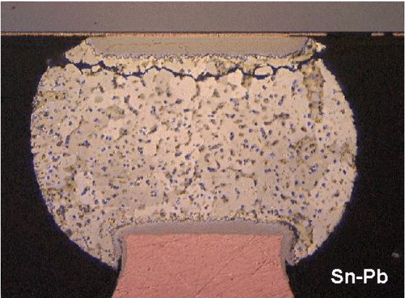
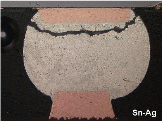
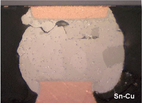
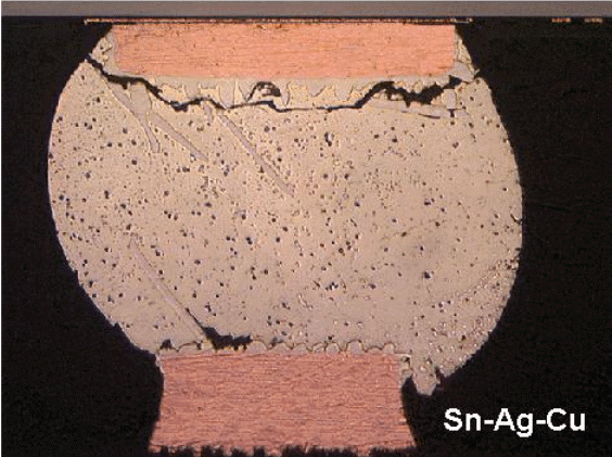
Figure 13. Optical micrographs of solder joint cross sections of solder joints on copper UBM/ Cu pads on organic substrates after thermal cycling at 0ºC–100ºC. |
||
|
|
||
The Sn-37Pb flip-chip interconnects fail by crack formation and propagation
through heterogeneous coarsened bands near the UBM/solder interface as shown
in Figures 13a, 13b,
13c, and 13d.
The heterogeneous coarsened region forms as a result of the strain concentrating
at the eutectic cell boundaries,31–33
which are slightly coarsened and are the weakest regions of the joint. Damage
accumulates at the cell boundaries and anneals at the high-temperature portion
of the thermal cycle, resulting in coarsening. Coarsening continues until the
tin and lead grains in the coarsened bands are so large that they can no longer
slide and rotate to accommodate the strain, resulting in grain-boundary crack
initiation and propagation. The UBM/solder interface is the highest strain region
in the joint and is where coarsening and failures typically occur for eutectic
tin-lead flip-chip interconnects. The cracks were observed to form on the outer
edge of the bump and propagate to the center of the bump. The surface of the
solder joint remains smooth after thermal cycling, indicating that the damage
was localized to the heterogeneous coarsened band.
The eutectic Sn-0.7Cu solder exhibited a failure mode that differed from the
other solder alloys studied. The initiation and propagation of fatigue cracks
is through the grain boundaries in the Sn-0.7Cu solder, as shown in Figures
13a, 13b,
13c, and 13d.
The fatigue cracks initiated on the highest point of strain on the bump, closer
to the edge of die, then propagated across the middle of the bump toward the
center of the die. After thermal cycling, the surface of the solder bumps is
no longer smooth. The Sn-0.7Cu solder deforms by grain-boundary sliding. The
cracks were observed to propagate at the grain boundaries, significantly removed
from the UBM/bump interface, near the center of the joint. This solder is the
most compliant in thermal fatigue and undergoes massive deformation before failing
by crack propagation.
The failure mode in ternary Sn-3.8Ag-0.7Cu solder on TiW/Cu UBM is significantly
different from that in Sn-0.7Cu. The thermal fatigue cracks initiated and propagated
at the intermetallics and intermetallic/solder interface, as shown in Figures
13a, 13b,
13c, and 13d.
The solder bump surface did not deform during thermal cycling nor did the microstructure
evolve. The fine colony and dendritic microstructure makes this solder bump
stronger and less compliant to thermal fatigue deformation than Sn-0.7Cu solder.
The strain imposed during thermal cycling is accommodated at the weak link of
the SnAgCu/UBM interconnect at the IMC/ solder interface. This failure mode
has a shorter fatigue life for Sn-3.8Ag-0.7Cu compared to Sn-37Pb or Sn-0.7Cu.
The failure behavior of Sn-3.5Ag solder is shown in Figures 13a,
13b, 13c,
and 13d. Similar to the Sn-3.8Ag-0.7Cu
alloy, the thermal fatigue cracks in the Sn-3.5Ag solder cracks initiate and
propagate through the intermetallics and at the intermetallics/solder interface.
The surface of the solder bump also exhibited no deformation with the damage
concentrated at the solder/intermetallic interface. The Sn-3.5Ag solder has
a shorter thermal fatigue lifetime than Sn-3.8Ag-0.7Cu, even though the failure
behavior appears to be similar. The only difference between the two alloys is
the microstructure of the Sn-3.5Ag bump appears to have more Ag 3 Sn intermetallics
present. It is hypothesized that the large Ag3Sn
intermetallic plates strengthen the joint, as shown in Figure
11, and further reduce the compliance of the solder, thereby shortening
the thermal fatigue life.
For the solders examined in this study, the shear strength has a direct correlation
to fatigue performance. The weaker, more compliant, and faster steady-state
creep rate solder (Sn-0.7Cu) has a longer fatigue lifetime. Eutectic tin-lead
has the same low shear strength as Sn-0.7Cu but has a shorter thermal fatigue
lifetime due to heterogeneous coarsening. It is well established that heterogeneous
coarsening concentrates strain in the joint to the coarsened band and accelerates
crack formation and propagation.31–33
The Sn-0.7Cu alloy undergoes massive deformation during thermal cycling. This
deformation protects the semiconductor device from damage due to imposed strain.
Interestingly, even with significant surface deformation, the crack formation
takes longer in Sn-0.7Cu than the other solders that had no surface deformation.
The Sn-0.7Cu accommodates the thermal strain by grain-boundary sliding and rotation.
The self-diffusion of tin to accommodate the sliding and rotation is sufficient
to delay the formation of cracks. An additional positive aspect of the Sn-0.7Cu
solder is that failure is only observed in the solder joint away from the brittle
intermetallic/solder interface.
Based on the results of this study, the optimal lead-free solder alloy for flip-chip interconnects is Sn-0.7Cu. The alloy contains no silver, so it is the lowest cost alternative of the lead-free alloys. The solder can be applied in either a paste form (for screen-printed bumps) or plated. The other lead-free solder alloys can only be plated with difficulty. Sn-0.7Cu has the highest melting temperature of the lead-free alloys proposed for flip-chip applications and, thus, provides some melting temperature hierarchy for subsequent package solder processing. The intermetallic structure of the lead-free alloys is similar to that of eutectic tin-lead. The interfacial intermetallics grow at a faster rate during reflow of the lead-free alloys, but, during solid-state aging, the lead-free solders have a slower intermetallic growth rate. Sn-0.7Cu has superior thermal fatigue performance of the lead-free alloys, surpassing that of the low melting temperature standard of eutectic tin-lead. For lower cost, ease of processing and superior thermal fatigue performance, Sn-0.7Cu is the optimal lead-free solder alloy for flip-chip interconnects.
The authors would like to acknowledge the support of Dr. Li Li, Jaynal Molla, and Owen Fay for solder bumping the test wafers.
1. N.C. Lee,
“Pb-free Soldering—Where the World is Going,” Advancing
Microelectronics (Sept./Oct. 1999), p. 29.
2. A. Grusd, “Integrity of Solder
Joints from Pb-Free Solder Paste,” Proc. NEPCON West ’99 (Norwalk, CT:
Reed Exhibition Companies,
1999).
3. J. Glazer, “Metallurgy of
Low Temperature Pb-Free Solder for Electronic Assembly,” Int. Mater. Reviews,
40 (2) (1995), pp. 65–93.
4. J. Glazer, “Microstructure
and Mechanical Properties of Pb-Free Solder Alloys for Low-Cost Electronic Assembly:
A Review,” J. Electron.
Mater., 23 (8) (1994), pp. 693–700.
5. G. Whitten, “Pb-free Solder
Implementation for Automotive Electronics,” Proc. 50th Electron. Comp. Tech.
Conf. (Piscatawny, NJ: IEEE
Publications, 2000), pp. 1410–1415.
6. E. Bradley, III and J. Hramisavljevic,
“Characterization of the melting and wetting of Sn-Ag-X Solders,” Proc. 50th
Electron. Comp. Tech. Conf. (in Ref. 5), pp. 1443–1448.
7. W.K. Choi and H.M. Lee, “Effect
of Soldering and Aging Time on Interfacial Microstructure and Growth of Intermetallics
Between Sn-Ag Solder and Cu substrates,” J.
Electron. Mater., 29 (10) (2000), pp. 1207–1213.
8. F. Guo et al., “Effects of
Reflow of Wettability, Microstructure, and Mechanical Properties in Pb-free
Solders,” in Ref. 7, pp. 1241–1248.
9. T.S. Choi, K.N. Subramanian,
and J.P. Lucas, “Thermomechanical Fatigue Behavior in Sn-Ag Solder Joints,”
in Ref. 7, pp. 1249-57.
10. Y. Miyazawa and T. Ariga,
“Microstructural Change and Hardness of Pb-free Solder Alloys,” Proc. 1st
Int. Symp. On Environ. Conscious Design (Los Alamitos, CA: IEEE
Comput. Soc., 1999), pp. 616–619.
11. M. Abtew and G. Selvardery,
“Pb-free Solder in Microelectronics,” Mater. Sci. and Eng., 27 (2000),
pp. 95–141.
12. H.K. Seelig and D. Suraski,
“The Status of Pb-free Solder Alloys,” Proc. 50th Electron. Comp. Tech. Conf.
(in Ref. 5), pp. 1405–1409.
13. K.G. Snowden, C.G. Tanner,
and J.R. Thompson, “Pb-free Soldering Interconnects: Current Status and Future
Developments,” Proc. 50th Electron. Comp. Tech. Conf. (in Ref.
5), pp. 1416–1419.
14. T.M. Korhonen et al., “Reactions
of Pb-free Solders with CuNi Metallizations,” in Ref. 7,
pp. 1194–1199.
15. J.C. Foley et al., “Analysis
of Ring and Plug Shear Strengths for comparison of Pb-free Solders,” in Ref.
7, pp. 1258–1263.
16. M.W. Roberson et al., “Conversion
between Standard and Low-alpha Pb in Solder Bumping Production Lines,” in Ref.
7, pp. 1274– 1277.
17. Z. Hasnain and A. Ditali,
“Building-in Reliability: Soft Errors-A Case Study,” 30th Annual Proc. Reliability
Physics (1992), pp. 276–280.
18. D.R. Frear and P.T. Vianco,
“Intermetallic Growth Behavior of Low and High Melting Temperature Solder Alloys,”
Metall. Trans. A,
25A (1994), pp. 1509–1523.
19. D.R. Frear et al., editors,
Solder Mechanics: A State of the Art Assessment (Warrendale, PA: TMS,
1990).
20. W.J. Boettinger et al.,
The Mechanics of Solder Alloy Wetting & Spreading (New York: Van
Nostrand Reinhold, 1993), Ch. 4.
21. H.K. Kim, K.N. Tu, and
P.A. Totta, “Ripening-assisted Asymmetric Spalling of Cu-Sn Compound Spheroids
in Solder Joints on Si Wafers,” Appl.
Phys. Lett., 68 (16) (April 1996), pp. 2204–2206.
22. S. Chada et al., “Cu Substrate
Dissolution in Eutectic Sn-Ag Solder and Its Effect on Microstructure,” in Ref.
7, pp. 1214–1221.
23. B. Roesner et al., “Thermal
Fatigue of Solder Flip-Chip Assemblies,” Proc. 48th Electron. Comp. Tech.
Conf. (Piscataway, NJ: IEEE
Publications, 1998), pp. 872–877.
24. M. Harada and R. Satoh,
“Mechanical Characteristics of 96.5 Sn/ 3.5 Ag Solder in Micro-bonding,” IEEE
Trans. on Comp, Hybrids, and Manuf. Tech., 13 (4) (1990), pp. 736–742.
25. J.J. Stephens and D.R.
Frear, “Time Dependent Deformation Behavior of Near Eutectic 60Sn-40Pb Solder,”
Metall. Trans. A,
30A (1999), pp. 1301–1313.
26. Z. Mei and J.W. Morris,
“Characterization of Eutectic Sn-Bi Solder Joints,” J.
Electron. Mater., 21 (1992), pp. 599–607.
27. D.R. Frear, Constitutive
Behavior of Pb-Free Solder Alloys, Sandia National Labs Report # SAND96-0037
(1997).
28. J. Liang et al., “Creep
Study for Fatigue Life Assessment of Two Pb-Free High Temperature Solder Alloys,”
Mater. Res. Soc. Symp. Proc., 445 (1997), pp. 307–312.
29. A. Grusd, “Integrity of
Solder Joints from Pb-Free Solder Paste,” Proc. NEPCON West’99 (Norwalk,
CT: Reed Exhibition Companies,
1999).
30. A. Grusd, “Lead Free Solders
in Electronics,” Proc. Surface Mount Int. Conf. (Edina, MN: Surface
Mount Technology Assoc., 1998), pp. 648–661.
31. D.R. Frear, D. Grivas,
and J.W. Morris, Jr., “Microstructural Study of the Thermal Fatigue Failures
in 60Sn-40Pb Solder Joints,” J.
Electron. Mater., 17 (1988), p. 171.
32. D.R. Frear, D. Grivas,
and J.W. Morris, Jr., “Parameters Affecting Thermal Fatigue Behavior of 60Sn-40Pb
Solder Joints,” J.
Electron. Mater., 18 (1989), pp. 671–680.
33. D.R. Frear, “Microstructural
Evolution During the Thermomechanical Fatigue of Solder Joints,” The Metal
Science of Joining, ed. M.J. Cieslak et al. (Warrendale, PA: TMS,
1992), pp. 191– 200.
D.R. Frear, J.W. Jang, J.K. Lin, and C. Zhang are with Interconnect Systems Laboratories at Motorola.
For more information, contact D.R. Frear, Interconnect Systems
Laboratories, Motorola, Tempe, AZ 85284;
(480) 413-6655; fax (480) 413-4511; e-mail darrel.frear@motorola.com.
Direct questions about this or any other JOM page to jom@tms.org.
| If you would like to comment on the June
2001 issue of JOM,
simply complete the JOM on-line critique form |
|||||
|---|---|---|---|---|---|
| Search | TMS Document Center | Subscriptions | Other Hypertext Articles | JOM | TMS OnLine |