This article reviews concepts and
techniques for performing instrumented
tensile testing of materials at small dimensions.
State-of-the-art methods to
probe tensile behavior of micro- and
nanoscaled materials span many orders
of magnitudes of force and displacement,
often requiring a custom solution
for each new material discovery. We
discuss the experimental opportunities,
challenges, and pitfalls in concert with
the scientific insights revealed from tensile
investigations at length scales
where conventional wisdom is challenged
on how materials deform.
INTRODUCTION
Developing mechanical tensile testing
techniques and methodologies of
materials in miniscule dimensions to
accompany the accelerating pace of
technological miniaturization has been
a challenging task. Novel device architectures
have been proposed that utilize
tiny building blocks (e.g., hybrid materials,
nanocomposites, microelectromechanical
systems [MEMS] and nanoelectromechanical
systems [NEMS]
materials, nanostructured thin fi lms,
nanoporous structures, nanowires, and
nanotubes) because of their superior
properties, even in the absence of a
complete understanding of the governing
mechanisms for deformation. The
race is on to uncover the mechanisms
that give rise to different properties
when atomic scales are approached and change
our thinking on how materials
deform. Yet, the accurate and reliable
testing at these length scales is shrouded
with uncertainty.
The following experimental questions
arise: How can we fabricate small
specimens with good geometric tolerances?
How do we measure the dimensions
of small samples that cannot be
imaged with conventional optical methods?
How can we measure and apply
small forces with high dynamic range?
How do we manipulate and grip small
specimens?
This article focuses on instrumented small-scale tensile (i.e., stretching or
pulling) testing approaches, where load
is applied uniaxially and the resulting
stress and strain state is nominally uniform
in the specimen. Simply stated,
micro- and nanotensile approaches differ
in comparison to other small-scale
methods in that the interpretation of
data is relatively straightforward, while
the technical hurdles can be high. Conversely,
techniques such as nanoindentation
are relatively simple to execute,
while the interpretation can be challenging.
TENSILE TESING APPROACHES AND TECHNIQUES
There are several experimental hurdles
that must be overcome to do proper
tensile testing of materials in order to
obtain precise mechanical property
measurements. In the macro-world, the
majority of these issues has been studied
in detail and in many cases standardized
(e.g., ASTM standards). The
pertinent questions at the micro- and
nanoscale become: What techniques
can we simply scale down from largescale
approaches, and at what point do
we need radically different methodologies
to deal with reduced dimensions?
The following sections systematically
address the steps necessary to realize a
tensile test at small scales and highlight
several unique approaches that researchers
in the field have developed to overcome
these challenges.
The synthesis of materials with reduced
dimensions (e.g., coating materials,
novel nanostructures, thin films) is
a burgeoning field of research. Metrology
for accurate sample measurement
and micro- and nanostructural characterization
must be juxtaposed with synthesis
and testing. These topics are deserving of their own attention (see, for
example, Reference 1), and major progress
has been made in the last decades;
advances have been made in marriage
with the development of novel microscopy
technologies. Here the emphasis
will be placed entirely on the issues and
challenges pertaining to mechanical testing of small-scale materials.
Specimen Harvesting,
Manipulation, and Gripping
Specimens at the larger end of the
length scales covered in this overview
(envelope dimensions of several mm ×
hundreds of μm × tens to hundreds of
µm, see, e.g., Figure 1) can be handled
in much the same way that conventional
tensile specimens are. Sharp tweezers
can often be used for manipulating
specimens, and more controlled air
tweezers for soft and ductile specimens.
In a recent review on microscale mechanical
characterization, K.J. Hemker and W.N. Sharpe2 highlighted techniques
for fabricating and handling
freestanding microspecimens and presented
examples of the insightful results
obtained from testing for a broad range
of materials applications.
However, many micro- and nanoscale
specimens are typically very fragile
and cannot withstand the brutality of
conventional handling tools (e.g., tweezers,
hands). Two general categories of
remedies are employed to accomplish
specimen handling: mounting the specimen
on a support structure that is large
and/or stiff enough to handle easily with
typical tools, and harvesting individual
specimens from the location where they
were grown, assembled, or dispersed
using micro- and nanomanipulators and
transferring them to a testing device.
Figure 1 illustrates examples of specimen
geometries as a function of size
and manipulation scheme.
A support structure can easily be integrated
into a microfabrication or MEMS
processing scheme in order to test freestanding
thin films. Both additive (e.g.,
deposition of layers on a substrate) and
subtractive (e.g., etching through layers,
removal of sacrificial layers) processes
can be used in the process flow
to implement a platform that consists of
a thin film that is anchored to a substrate
but released in the gage section. C.A.
Neugebauer3 developed such a method
using gold films and a rock salt substrate
as far back as 1960. D.T. Read and J.W.
Dalley,4 and later W.N. Sharpe, Jr. and
colleagues,5 extended this technique
for testing films that are deposited on
a silicon substrate. As shown in Figure
1, a freestanding polysilicon thin film
specimen (3 μm thick) is framed by a
silicon supporting structure consisting
of 500 µm thick silicon grips and support
strips on the periphery.5 This die is
handled easily with tweezers, and can
be integrated into a tensile testing platform.
Prior to testing, the support strips
can be cut with a diamond-impregnated
rotary tool so that the loads are only incurred
by the thin film. This technique
has been successfully utilized for the
testing of Ti-Al-Ti,4 polysilicon,6 nanocrystalline
aluminum,7 gold,8,9 SiN,10
and SiC.11
An alternative method involves surface
micromachining of thin-film materials
on the surface of a substrate
and subsequently removing sacrificial
layers or etching below specimens to
release the gage section, as introduced
by T. Tsuchiya et al.12 Figure 1 shows
the so-called narrow thin-film specimen
geometry of W.N. Sharpe et al.13 One
end of the specimen remains anchored
to the substrate, while the other consists
of a large paddle with arrays of patterned
etch holes that allows for release
from the substrate during etching. This
paddle is attached to anchors that can be
cut before testing using a sharp micromanipulator.
The large paddle can be
gripped electrostatically12 or by gluing
a stiff fiber and attaching the other end
to a load cell.1317 One advantage of this
method is the ability to test specimens
in a more parallel fashion, since the
alignment of the loading device needs
to be accomplished only once per die.
D.T. Read et al.18 proposed an alternative
paddle geometry that has been used
by others19,20 consisting of an annular
ring on the free side of the specimen,
allowing for a separate hook structure
to apply forces to the specimen.
Co-fabrication of the specimen and
testing apparatus has been proven to be
an attractive strategy in situations where
the materials synthesis can be integrated
in the device process flow. This is particularly
appealing for materials used in
microelectronics, MEMS, and NEMS
synthesized by vapor deposition methods,
and allows for batch processing
and testing of many specimens on a single
wafer. Co-fabrication has the clear
advantage of circumventing gripping
and alignment issues by incorporating
the specimen into the device fabrication
using multiple photolithography masks,
for example. M.A. Haque and M.T.A.
Saif have co-fabricated and performed
tensile testing of thin metal films as thin
as 30 nm21 and H.D. Espinosa and colleagues
have employed this strategy to
test polysilicon specimens and one-dimensional
(1-D) nanostructures.22
The described strategies for specimen
manipulation are not always feasible
when a specimens largest dimension
is less than several tens of micrometers,
as in the case of nanotubes, nanowires,
nanobelts, and some biomaterials. Y.
Zhu, C. Ke, and H.D. Espinosa23 recently
reviewed the state of the art of
mechanical characterization of 1-D
nanostructures, and point out that one
of the largest challenges is the handling
of extremely small specimens. Microand
nanomanipulators can be used in
conjunction with high-resolution imaging
systems to locate, attach, transfer,
and manipulate these structures to the
desired testing platform. For example,
several commercial nanomanipulators
with multiple degrees of freedom are
now available that make use of piezoelectric
materials combined with socalled
inertial drive mechanisms. These
actuators exploit the difference between
the static and dynamic coefficients of
friction, offering sub-nanometer resolution
with millimeter to centimeter ranges
(examples of commercially available
systems include Kleindiek Nanotechnik,
Omniprobe, and Klocke Nanotechnik).
By attaching fine tapered probes
(typically sharpened by electropolishing,
and many times re-sharpened by
the focused ion beam [FIB]), tiny specimens
can be manipulated and harvested
with no to minimal handling damage.
In situations where specimens can no
longer be imaged using white-light optical
microscopy, nanomanipulators can
be integrated into transmission electron
microscopy (TEM),24,25 scanning electron
microscopy (SEM), and/or FIB26
environments where they can be used
in conjunction with local deposition
systems for specimen attachment.
Common approaches for in situ attachment
include local deposition or accumulation
of hydrocarbons present in the
vacuum system using a focused e-beam
(EBID),27 or the local injection of a precursor
gas (called a gas injection system,
or GIS) that adsorbs to the sample
surface and can be locally decomposed
using EBID or an ion beam (IBID). The
desired compound is deposited where
the beam is scanned, and the reaction
products are volatile and can be pumped
away. This method has been utilized extensively,28,29 and GIS systems currently
exist with the capability of depositing
gold, platinum, and tungsten. The GIS
method has also been used for local
metal deposition to grip specimens for
tensile testing. For example, S. Orso et
al. used IBID to deposit fixation tape
of tungsten to individual setae from the
leg of a beetle for subsequent tensile
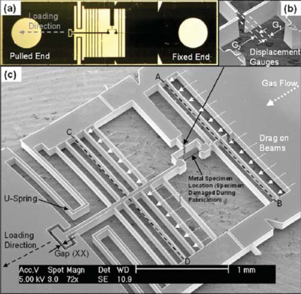
testing.30 Figure 2 shows the manipulation
and transfer of nanowires by utilizing
a commercial nanomanipulator and local platinum deposition. Limited information
exists regarding the strength
of these tape deposits given that the
microstructure and corresponding properties
vary wildly depending on the deposition
conditions.31 Nevertheless, this
gripping method has proven to be sufficiently
strong for specimens as large as
several micrometers, generating forces
as high as ~ 5 mN.30
In addition, the advent of atomic force
microscopy (AFM/SPM) based techniques
has spawned a new generation
of tools using the atomically sharp tip
as an end effector to manipulate objects
as small as individual atoms.32 This approach
is often named the AFM nanorobot33,34
and can be made more versatile
by functionalizing the tip to enhance the
specificity of binding to certain molecules
or particles (often called chemical
force microscopy). For example, S.H.
Leuba et al. employed this approach to
stretch single strands of chromatin and
measured their mechanical response.35
Novel manipulation and patterning
techniques have been proposed and
could prove to be very useful for attachment
of tensile specimens, particularly
those that require high throughput or
special environments (e.g., aqueous solutions,
non-ambient conditions). Some
examples include random dispersion of
nanostructures in suspension solution
onto patterned grids or by directed selfassembly
to encourage pattern formation,23 alignment using external electric
fields by utilizing the dielectrophoresis
effect,36,37 and direct growth of nanostructures
by patterning or manipulating
growth catalyst particles in desired
locations and orientations.38,39 These
methods show promise for accelerated
tensile testing of materials to efficiently
generate large materials properties datasets.
Actuation and Force/
Displacement Measurement
One must consider the expected
forces and displacements that would be
incurred when approaching micro- and
nanoscale tensile testing (see Figure 3
for literature values of force and displacement
ranges for a variety of testing
approaches4044). Other important
considerations when choosing a testing
apparatus are the materials properties
that are desired (e.g., elastic moduli,
yield strength, stress relaxation, etc.)
and whether dynamic material changes
(e.g., discrete deformation, yield
points) are expected during testing. At
larger scales, Sharpe, Hemker, and coworkers2
showed that many microtensile
testing needs can be satisfied using
careful selection of commercially available
components.
Actuation technologies exist that offer
nanometer and sub-nanometer resolution,
and others are available that offer
large ranges of motion; the challenge is
obtaining a system that provides high
dynamic range (i.e., fine step sizes and
large ranges). Piezoelectric actuators
offer decided advantages in terms of
resolution of motion (since the principle
is based on atomic-level straining) and
speed control, and can be fabricated in
special stack geometries to extend the
range of motion. However, piezo-based
actuation systems are susceptible to direct
current (DC) drift and stack designs
are not always very compact, precluding
use in restricted spaces (e.g., in situ
experiments). High dynamic range actuators
are commercially available that
make use of the inertial drive mechanism
mentioned previously, combining
precision motion of piezoelectric
materials with large travel (e.g., tens
of millimeters). This motion can be accomplished
using linear sliding or by a
ratcheting motion of piezoelectric jaws
over a finely threaded screw.
Thermal actuation has been demonstrated
as a useful and stable actuation
method,45,46 which involves the coupling
of electrical, thermal, and mechanical
fields. A DC current is passed between
external contacts connected to slender
beams, which induces resistive heating
along angled beams. The heat resulting
from the Ohmic dissipation results in
thermal expansion of the beams along
their longitudinal axes and projects
into rectilinear motion for actuation.
The amount of force and displacement
that the thermal actuator can generate
is a function of the beam geometry, the
angle of inclination relative to the actuation
axis, the number of beams used,
and the material properties of the actuator.
Once the actuation technique has been
chosen, one must consider a method for
measuring the tiny forces encountered
in small-scale specimens. Many commercial
load cells based on conventional
technology such as Wheatstone bridges
or internal leaf springs are available
that provide the capability of measuring
forces as small as several tens of
micronewtons.
Flexure-based load measurement systems
that rely on transverse deflection
of beams perhaps offer the most versatility,
since the load range can be customized
to suit the testing needs simply
by adjusting the geometry. This can be
accomplished readily at larger scales
by using CAD-based EDM or laser cutting
methods, and by microfabrication
or FIB milling at smaller length scales.
Cantilevered beams are sensitive load
sensors since they are very compliant;
indeed, this point is exploited in AFM,47
surface stress-induced chemical and biological
sensing,48 and stress evolution
studies during thin-film growth.49 For
example, M.F. Yu et al.50 used two opposing
AFM cantilevers to manipulate
and test multi-walled carbon nanotubes
in tension. S. Gudlavaletti and colleagues51
demonstrated the versatility
of flexure-based systems by providing
design considerations and constructing
monolithic apparatuses to perform tensile
testing at different length scales.
Several researchers promoted this
technique for force measurement during
tensile testing of one-dimensional
nanostructures,22,23,52 freestanding metallic
thin films,21,53 and polysilicon22
by microfabricating testing devices that
integrate actuators and load measurement
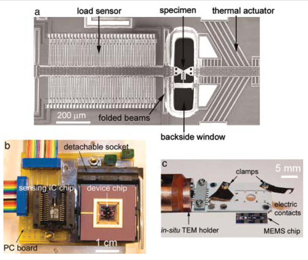
devices all on a single chip. Haque
and Saif21 introduced an integrated testing
device consisting of silicon beams
and grips that are etched through the
entire chip in order to perform in situ
TEM tensile testing. They developed a
new generation of testing platform,54 as
shown in Figure 4a, with some advantages
including reference markers for
relative displacement measurements
(thus, 1-D strain) and the possibility for
concurrent four-point electrical characterization.
This device can be integrated
easily into existing TEM straining holders
and simple ex situ actuators, but requires
external loading. Espinosa and
co-workers22 developed fully integrated
testing platforms that rely on thermally
driven actuators or capacitive structures
inducing electrostatic forces (Figure
4b). Their devices require only that electrical contacts be made to the device,
which can be easily accomplished using
standard wire bonding. R.S. Ruoff et al.55
designed and implemented a flexure based,
microfabrication-realized testing
platform with a novel geometry that
produces displacement de-amplification
from thermal actuators, resulting in
precise nanometer-level control.
Nanoindentation systems are most
often utilized for compression testing of
materials (e.g., sharp indentation, pillar
compression), but can also be utilized
for small-scale tensile testing.52 Some
transducer designs rely on electromagnets
for force actuation and capacitive
systems for displacement measurement
(see for example Reference 56 for a
review on instrumented indentation),
while others utilize electrostatic interactions
between capacitive structures
for force generation.57 The latter systems
employ a three-plate capacitor
design and superimpose high-frequency
antiphase alternating current (AC)
signals to opposing capacitor plates to
measure displacement.57 It should be
noted that both transducer designs are
inherently force-controlled, but sophisticated
feedback systems can be used
to achieve quasi-displacement control
during testing.
Focused light can also be used to apply
or measure forces on small specimens.
The research group of C. Bustamante58
implemented an optical trapping
system (also known as optical tweezers)
to experimentally investigate the extensibility
of DNA. This approach exploits
the electrical field gradient produced
by a focused laser beam, which interacts
with and traps dielectric particles
(typically glass or polymeric beads attached
to biomolecules) in the center of
the beam. If the bead is moved from the
optical center, then a restoring force is
applied to the dielectric particle due to
the momentum transfer from the scattering
of light, allowing for mechanical
testing experiments. Position-sensitive
detectors (e.g., photo diodes or CCD
cameras) are placed downstream from
the optical path and can detect beam
displacements (at the nanometer level),
while forces (as low as 1013 N) are applied
by either steering the beam or by
precisely moving the other end of the
specimen using a piezoelectric stage.59
It should be noted that careful and tedious
calibration of these systems is
necessary to quantify the changing trap
stiffness and displacement output.60
Strain Measurement
Accurate tensile testing requires direct
strain measurement in the gage
section61 of the specimen and in small-scale
testing this can be achieved by
non-contact strain measurement methods.
Notable approaches include the interferometric
strain displacement gage
(ISDG62), tracking of diffraction spots
from gratings deposited on specimen
surfaces,63 digital image correlation
(DIC),16,64 and differential digital image
tracking (DDIT).15,30 These techniques
also allow for the measurement of the
lateral strain to measure Poissons ratio.5,65 Digital image correlation and
DDIT have the advantage of full-field
capability giving local fidelity (e.g.,
strain heterogeneities near grain boundaries).66 These techniques measure the
strain even after tensile necking extending
the measurable stress-strain behavior
beyond the maximum engineering
stress.65 In the case of in situ tensile testing,
DIC and DDIT are ideal methods
for strain measurement, as the SEM,6668
FIB,30 or AFM16 can be used as image
sources during the test. Thus, quantitative
information can be extracted in addition
to imaging the deformation morphology during testing.
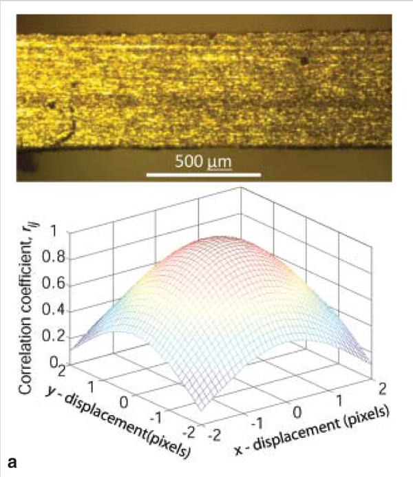
The basic premise of DIC is as follows,
and a representative image demonstrating
good surface contrast on a
microspecimen is shown in Figure 5a.
The correlation coefficients of subsets of
consecutive images (typically between
10 × 10 to 40 × 40 pixels2) are calculated
and plotted versus their position. Biquadratic
functions, for instance, can be
used to locate the maximum correlation
coefficient (with sub-pixel resolution)
that is representative of the optimal fit
between the subsets of the two images
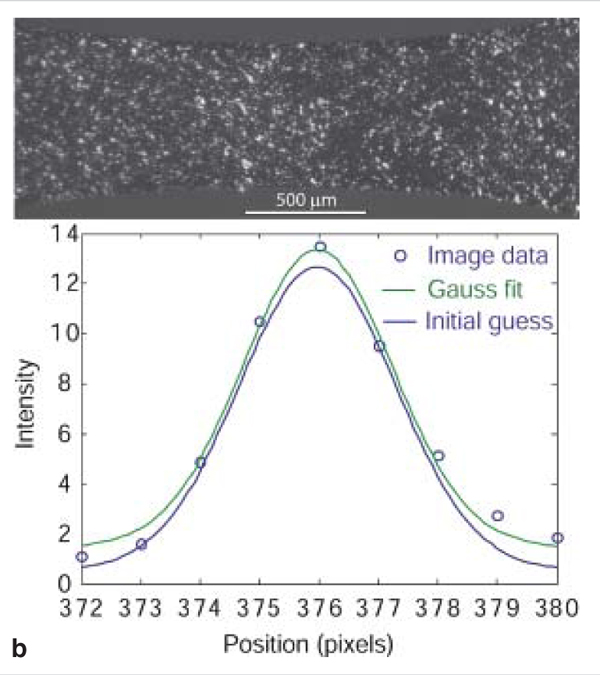
(Figure 5a). Differential digital image
tracking requires intensity peaks in the
source images that can be tracked by a
peak fitting algorithm (Figure 5b). This
method can achieve a resolution of up
to a thousandth of a pixel, which allows
for good strain fidelity even in the
absence of many pixels (e.g., AFM images
with ~200 × 200 pixels2 resulting
in strain resolutions of up to Δε = 105).
Ultimately, the resolution of DIC and
DDIT primarily hinge on the noise present
in the imaging system. Differential
digital image tracking is typically less
susceptible to local image noise since
features are tracked that span multiple
pixels. Free MATLAB® code for DIC
and DDIT is available online.69
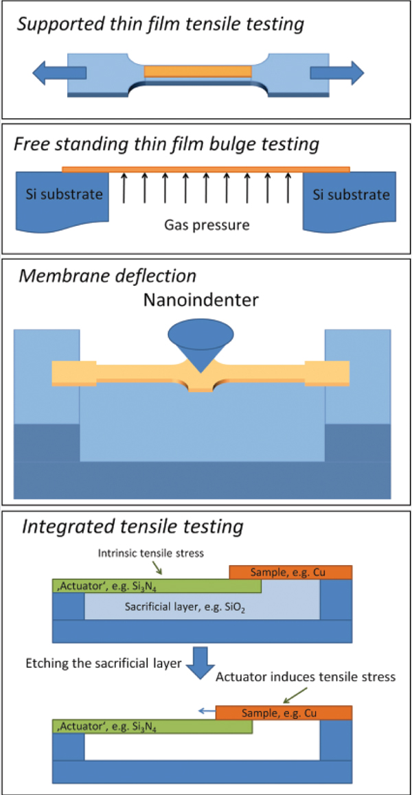
Indirect Tensile Testing Methods
The focus of this paper is on instrumented
tensile testing in which the
uniaxial load and displacement are
measured directly and independently.
However, several small-scale testing
methods have been reported that induce
tensile loads in specimens and are
capable of measuring full stress-strain
curves. Notable examples include
plane-strain bulge testing,70 the membrane
deflection technique,71 and an onchip
residual stress-induced actuation
method.72 These methods are illustrated
in Figure 6.
Co-deforming a thin film with a polymer
substrate (Figure 6) is another way
to stabilize fragile specimens and is also
of technological interest for use in flexible
electronics for displays and active
textiles. Several researchers have utilized
this approach to study the tensile
behavior of films as thin as 20 nm.7377
Furthermore, in situ x-ray diffraction
can be used to quantify stress evolution
in crystalline materials since the total
force cannot be directly related to stress
in the thin film. Upon analyzing the diffraction
patterns, one can calculate the
elastic multi-dimensional lattice strains
from interplanar crystalline spacings
and combining multiple measurements
in orientation space. These quantities
can be related via careful analysis to the
stress in the crystal via the elastic constants.78,79 The influence of Poisson contraction
and time-dependent relaxation
of the underlying polymer can therefore
be mitigated as employed extensively
by H. Hommel and O. Kraft,73 P.A. Gruber
et al.80,81 for continuous films and S.
Olliges et al. for structured films.82
Bulge testing involves pressurizing a
freestanding thin film that is clamped at
its edges to induce tensile stresses in the
membrane (Figure 6); the pressure and
deflection of the membrane are measured
independently, as introduced by
J.J. Vlassak and W.D. Nix.70 This has
been applied to the testing of various
metal films with and without passivation
layers.83,84
The membrane deflection technique
was developed by H.D. Espinosa and
colleagues,71,85 where a long doubly
clamped freestanding thin film is pushed
in its center using a nanoindenter (Figure
6). Given the lack of bending stiffness
in thin films, the transverse loading
translates to tension in the membranes
on either side of the loading point.
Force is measured by the nanoindenter, and the vertical deflection can be measured
using an interferometer.
Lastly, N. André et al.72 developed a
tensile testing technique which can be
integrated into a MEMS or microelectronics
process, where the actuation is
carried out by residual stresses in SiNx.
During etching of a sacrificial layer
that initially holds the layers in place,
the intrinsic stress in the SiNx actuator
pulls on the sample as illustrated in
Figure 6, and by integrating several of
these structures with different actuator
lengths, the actuated displacement can
be varied. The load on the sample can
be measured by the difference in displacement
of each actuator compared to
a stress-free state. Each actuator-sample
structure represents one data point on
the stress-strain curve.
INSIGHTS GAINED FROM SMALL-SCALE TENSILE TESTING
Micro- and nanotensile testing have
helped further our understanding of how
small volumes of materials deform, as
shown in the following examples.
Tensile Testing of Biological
Attachment Devices
Biologically inspired adhesion systems
have recently attracted significant
attention as a replacement for chemistry-
based adhesives, tapes, and industrial
grippers. Some insects and geckos
use hierarchical hairy attachment systems
of brush-like structures as small
as 200 nm to reversibly adhere to walls
and chase down their prey. Several
researchers have shown that van der
Waals interactions and capillary forces
provide the observed adhesion8689 and
have studied the related scaling laws.
The findings can be used to identify
the optimum geometric and materials
properties via adhesion maps.90,91 Measurements
of the mechanical properties
of these small structures is necessary
for efficient design yet challenging, as
the diameters of setae scale from several
micrometers down to 200 nm with
lengths between several micrometers
and 100 μm.
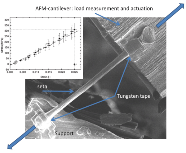
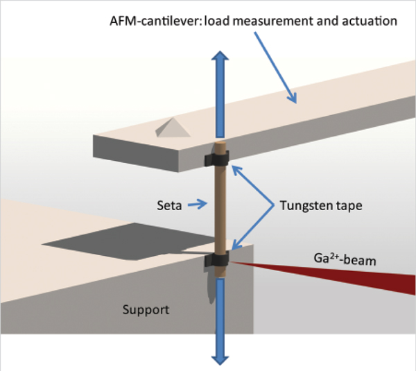
Orso et al.30 were successful in utilizing
a micromanipulator mounted into
an FIB microscope to separate, cut, and
fix single setae from the leg of a gastrophysa
viridula (beetle) and carry out
in-situ microtensile tests. The experimental
setup for tensile testing is shown
in Figure 7. The load was measured by
an AFM tip attached to the micromanipulator
and the setae were glued by
tungsten tapes deposited using IBID
to a metal block and the AFM tip. The
strain was calculated using DDIT from
the FIB micrographs obtained continuously
throughout the test.
The measured Youngs modulus
of the gastrophysa viridula setae was
13.3 ± 1 GPa and the reported ultimate
strength was 310 ± 60 MPa. The mechanical
behavior showed almost ideal
elastic behavior (inset of Figure 7) and
compares with properties of chitin fiber reinforced
composite materials. The
authors pointed out that the Youngs
modulus of biological materials is often
higher in vacuum than under normal
atmospheres due to dehydration. This
study set a precedent for extracting the
properties of biological attachment systems,
which aids designers in selecting
bio-mimicking materials and optimizing
structural design for the development
of artificial attachment systems.
Size-Dependent Plastic Behavior
in Single-Crystalline Metals
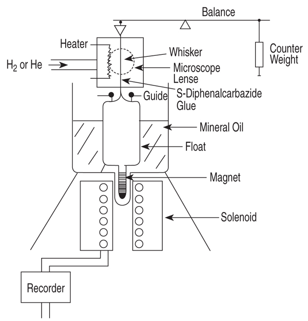
More than fifty years ago, S.S.
Brenner92 published seminal work on
the deformation of microscale single
crystals to convincingly demonstrate
that size indeed does matter, and deformation
behavior of metals can be
altered by simply changing the external
specimen size. He reported tensile
testing results of copper, iron, and silver
whiskers ranging in diameter from
approximately 1 μm to 15 μm and
1 mm to 4 mm in length that were
grown using reduction of halides and
tested in the apparatus shown in Figure
8a. Stress-strain behavior was characterized
as strong, but with limited
plastic flow, and pronounced deviations
from linear elasticity were measured
in the iron whiskers that were attributed
to strains that exceeded the linear
elastic limit of Hookian elasticity.92 He
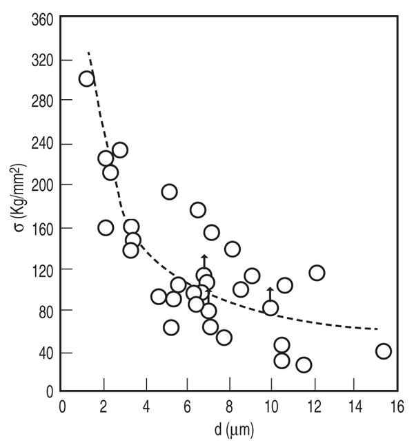
showed that the ultimate strength of the
whiskers showed prominent size dependence
(Figure 8b), with critical resolved
shear strengths falling closely to
the lower estimate for the ideal strength
of these metals in the case of the smallest
whiskers.
Brenner followed up this work93,94
with more results on copper, silver, and
gold whiskers using a modified setup
that prevented the load train from exhibiting
large deflections at the point of
a large excursion event. This improvement
allowed for the elucidation of
sharp yield points, followed by regions
of easy glide at a fraction of the yield
point stress (as little as 10%) that was
characterized by Lüders band propagation.
Interestingly, the yield point
exhibited size dependence, while the
lower flow region did not. These observations,
coupled with experiments that
showed that a fractured whisker with
less volume could be re-tested to recoup
an even higher yield point, indicated
that these whiskers had minimal
starting defects and extreme stresses
were required to nucleate defects. The
nucleation stress was dependent on the
probability of finding a critical defect of
a critical size; thus, the measured volume
or surface area dependence, akin
to the classic experiments on the deformation
of glass rods.95 The results of
this work highlighted the importance of
discrete defects in small volumes, catalyzing
the mantra of smaller is stronger,
a departure from our conventional
wisdom of continuum descriptions of
plasticity.
Recently, micro- and nanocompression
has been developed by M.D. Uchic
and colleagues96,97 to study size-dependent
(e.g., intrinsic and extrinsic size
effects) and site-specific (e.g., local
properties of composites, multi-phase
materials, etc.) properties of materials,
as discussed in a companion paper in
this issue. This approach makes use of
an FIB to fabricate small structures with
control of size, and experimental studies
on the deformation of face-centered
cubic (fcc),96,98102 body-centered cubic
(bcc),103,104 and amorphous metals105107
have been conducted. Crystalline metals
have shown a clear size dependence
on the yield or flow stress. A vigorous
debate has taken place to explain the
underlying deformation mechanisms
responsible for the size effect and departure
from bulk behavior that have
been revealed by this technique. The
prevailing mechanistic explanations
for fcc materials invoke the importance
of dislocation source nucleation and
activation,99 source truncation by free
surfaces and subsequent exhaustion,108
and dislocation starvation of defect free
crystals.109 These compression
experiments have revealed significant
insight on the deformation of small
metallic volumes, but the effect of the
compressive loading modality (e.g.,
heterogeneous stress state from column
tapering, stress concentrations arising
from friction between the punch and
the specimen, poorly defined boundary
conditions) on the observed size effect
is still elusive.
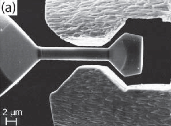
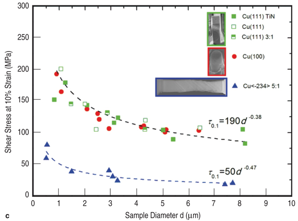
Recently, D. Kiener and colleagues110,111
and Uchic et al.97 developed
in situ SEM methods for tensile
testing of single-crystalline metallic
specimens fabricated using FIB methods.
The specimen and gripping configuration
from Kiener et al. is shown in
Figure 9, and was used for tensile specimens
with sizes ranging from 0.5 μm to
8 μm. The major finding of this work is
that tensile specimens with aspect ratios
(length to width ratio) of 2:1 or higher
exhibited yield strengths that were approximately
three times lower than
equivalent compression experiments
using the same FIB parameters and
experimental testing apparatus (Figure
9c). An extension of this work110 demonstrated
that reversing the loading of a
tensile specimen into compression does
not alter the yield strength; no tension compression
asymmetry was measured
in these specimens. However, lowering
the aspect ratio of the tensile specimens
to mimic that of the compression pillars
returns the strength to that measured
from compression. Moreover,
pronounced hardening is measured for
low-aspect-ratio specimens. This point
is attributed to the interaction and constraint
of dislocation glide planes with
the boundaries of the specimen, which
will induce dislocation pile-ups leading
to measurable hardening and a size
dependence of the strength. Taken as
a whole, these experiments emphasize
the importance of boundary conditions,
particularly in single-crystal deformation,
and inspire the need to deconvolute
the role of testing artifacts from
intrinsic size-dependent response.
A bridge between the experiments of
Brenner and the micro- and nanocompression
and microtension experiments
of specimens fabricated using the FIB is
still missing, given that microwhiskers
demonstrated strengths close to the ideal
strength while similarly sized specimens
fabricated using the FIB show
strengths significantly far away from
this upper bound. Recent experiments
from H. Bei and colleagues112 provide
evidence to suggest that the difference
in measured strength lies primarily on
the pre-existing defect structures in the
material. In those works, molybdenum
alloy compression pillars were fabricated
by directional solidification of
a eutectic and subsequent etching of
the matrix, and no use of the FIB was
needed. These pillars were presumably
defect-free and demonstrated strengths
near the calculated theoretical strength
of molybdenum and no size dependence
was measured. Size-dependent behavior
and lower strengths returned when
these specimens were irradiated with
the FIB using conditions that emulate
pillar preparation,113 or when the composite
material was pre-strained prior to
etching and testing of the molybdenum
alloy pillars.114 Recent experiments by
G. Richter et al.52 reporting tensile testing
of defect-free copper nanowhiskers
complement the experiments of Bei and
Brenner, also show a departure from
pillar behavior, and give strengths at
or near the ideal strength. The emerging
picture suggests that the presence
or absence of pre-existing defects in
small volumes greatly contributes to
the measured mechanical response of
the material, and points to the need for
thorough nanostructural characterization
to accurately predict deformation
and strength.
Deformation Mechanisms in
Nanocrystalline Metals
Small-scale tensile testing has also
made significant gains toward the understanding
of deformation behavior
of nanocrystalline metals, where the
internal length scale given by the grain
size defines the mechanical response.
It is now generally accepted that nanocrystalline
metals exhibit high strength
and limited ductility in comparison
with their coarse-grained counterparts,
and conventional dislocation descriptions
of crystal plasticity are abated
when the grain size is reduced below
approximately 100 nm. Elucidating the
new mechanisms to accommodate plasticity
that take over at reduced length
scales has been the subject of vigorous
research activity, along with several
reviews (see, for example References
115117). Proposed mechanisms that
contribute to measurable global plastic
strains include partial dislocation emission
and subsequent absorption from
grain boundaries, deformation twinning,
grain boundary sliding, enhanced grain
boundary diffusion, and grain boundary
migration. The common denominator
in all of these processes is that the large
fraction of interfaces plays a large role
in governing deformation.
Microtensile testing has been instrumental
in characterizing the mechanical
behavior of nanocrystalline metals,118120 primarily since large, fully
dense volumes of these materials are
difficult to synthesize, thus precluding
the use of conventional tensile testing.
For example, microtensile testing
coupled with post-mortem TEM118 and
in situ x-ray diffraction119 revealed that
plastic deformation in nanocrystalline
aluminum and nickel does not leave
stored dislocation content in the interior
of the grain as one would expect in microcrystalline
materials. These studies
helped form the currently accepted wisdom
that grain boundaries serve as both
the source and sink for dislocations in
nanocrystalline metals.
In parallel, nanostructured materials
are encountered in many thin film,
MEMS, and NEMS applications, as the
film deposition methods often synthesize
material with nanoscaled grains.
Freestanding thin film microtensile testing
has been employed to measure yield
strength, elastic moduli, hardening, and
ductility of vapor-deposited nanocrystalline
materials.7,63 Room-temperature
mechanical characterization of freestanding
submicrometer aluminum thin
films with thicknesses between 100 nm
and 400 nm by D.S. Gianola and colleagues7,65,121
have demonstrated that
nanostructures can be unstable under
the influence of stress, even those that
demonstrate good thermal stability.
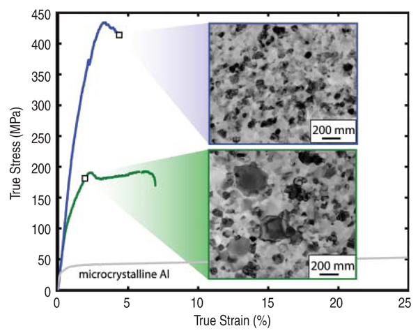
Two general classes of deformation
were uncovered as shown in Figure 10,
briefly characterized as either strong
with limited ductility and a stable microstructure
or intermediate strengths
with extended ductility and an evolving
microstructure. The occurrence of
stress-driven high-angle grain boundary
migration was correlated to the content
of impurities present during deposition.122 Characteristics of the growth
were not commensurate with conventional
descriptions of grain growth123
and instead appear to be in line with the
notion of shear stress-driven coupled
motion of both high- and low-angle
grain boundaries, as postulated by J.W.
Cahn and co-workers.124,125
CONCLUSIONS
Tensile testing at small size scales
is an attractive field of research and
technology since the output is directly
interpretable, without recourse to complex
models. Experimental techniques
have advanced and become commercially
available, enabling instrumented
testing in an increasingly controlled
manner. The most important developments
are the availability of easy-to-use
non-contact strain measurements and
small scale actuators and transducers,
combined with sensors of high fidelity
and dynamic range.
Ultimately, engineers of all disciplines
want predictive models of physical
phenomena. Extracting materials
properties across the length scale spectrum
will give us physically based and
technologically relevant models. Understanding
the fundamental response
of the building blocks of complex systems,
coupled with a good understanding
of physical constraints, will allow
for the possibility of true predictive
capability and intelligent engineering
design. Equipped with the hierarchical
knowledge of deformation at all length
scales, one can push the limits of materials
properties space126 by synergistically
combining materials behavior in a
hybrid manner.
OUTLOOK
While the design of small-scale applications
can often be based solely
on elastic and plastic properties drawn
from tensile testing, requirements during
lifetime will be multi-faceted and
lifetime can only be predicted if we understand
the physical mechanisms at all
scales. The various stimuli are inherently
coupled and the materials properties
should be measured in environments
that emulate real use (e.g., integrated
circuits, photovoltaics, fuel cells, advanced
batteries). Short diffusion paths, multiaxial stress states, cyclic loading,
and elevated temperature have distinct
implications at different length scales
and generate the need for intensive investigations.
Fatigue in pure thin films
has been under investigation for some
time now127129 and studies have found
that thinner films can show higher
lifetimes, which is a promising result.
Tensile testing at elevated temperature
is still limited although MEMS materials
have been tested,130 but reliable
temperature control is still challenging
and new concepts are needed if one
desires creep testing. Advancements
in coupled mechanical measurements
techniques (e.g., coupled with thermal,
electrical, photonic, or chemical loads)
at small length scales are promising and
represent an exciting arena for research.
Transient tests do offer the opportunity
to probe thermally activated processes
and can generate new insights on active
defect mechanisms.
Round-robin tensile tests, in which
multiple laboratories with distinct testing
capabilities collaboratively test
batches of specimens to interrogate the
uncertainty of measurement techniques,
offer a possibility to formulate testing
protocols and standardization. Tensile
techniques at decreasingly small scales
are still in development stages, but the
ultimate goal should be to achieve testing
standards commensurate with those
at larger scales. Research laboratories
should unite to ensure reliable and repeatable
results.
Many systematic small-scale tensile
testing studies have converged to the
following answer: The elastic properties
of fully dense microspecimens are
similar to those of their bulk counterparts,
as long as the effects of texture,
anisotropy, and porosity are properly
accounted for (see, for example, polysilicon
used in MEMS2). Conclusive
experimental evidence that demonstrates
the effects of surface stress on
both the elastic and plastic properties of
materials with nanometer dimensions is
elusive. Careful and systematic tensile
testing can offer significant insight here
and represents a direct way of measuring
such effects.
ACKNOWLEDGEMENTS
The authors would like to thank the
cast of characters that inspired their
interest in small-scale mechanical testing;
in particular our mentors Kevin
J. Hemker and William N. Sharpe, Jr.,
from whom we learned the science and
art of microtensile testing. C.E. would
like to acknowledge financial support
from the Deutsche Forschungsgemeinschaft.
D.S.G. acknowledges support
from an Alexander von Humboldt Postdoctoral
Fellowship.
REFERENCES
1. Y. Gogotsi, editor, Nanomaterials Handbook (Oxford,
U.K.: Taylor and Francis, Inc., 2006).
2. K.J. Hemker and W.N. Sharpe, Annual Review of
Materials Research, 37 (1) (2007), pp. 93126.
3. C.A. Neugebauer, Journal of Applied Physics, 31 (6)
(1960), pp. 10961101.
4. James W. Dally and David T. Read, JMR, 8 (1993),
pp. 15421549.
5. W.N. Sharpe, Jr. et al., Micro Electro Mechanical
Systems, 1997 (MEMS 97) (Piscataway, NJ: IEEE,
1997), pp. 424429.
6. K.J. Hemker et al., Journal of Microelectromechanical
Systems, 10 (3) (2001), pp. 317326.
7. D.S. Gianola et al., Acta Materialia, 54 (8) (2006),
pp. 22532263.
8. R.D. Emery and G.L. Povirk, Acta Materialia, 51 (7)
(2003), pp. 20672078.
9. W.N. Sharpe et al., unpublished work (2008).
10. R.L. Edwards, G. Coles, and W.N. Sharpe, Jr., Experimental
Mechanics, 44 (1) (2004), pp. 4954.
11. C.A. Zorman et al., Journal of Microelectromechanical
Systems, 14 (4) (2005), pp. 664672.
12. T. Tsuchiya et al., Micro Electro Mechanical Systems,
1997 (MEMS 97) (Piscataway, NJ: IEEE, 1997),
pp. 529534.
13. W.N. Sharpe, K.T. Turner, and R.L. Edwards, Experimental
Mechanics, 39 (3) (1999), pp. 162170.
14. W.N. Sharpe et al., Proceedings of IMECE 2006, 2006 ASME International Mechanical Engineering
Congress and Exposition (New York: ASME, 2006), p.
13290.
15. W.N. Sharpe et al., Experimental Mechanics, 47
(5) (2006), pp. 649658.
16. Ioannis Chasiotis and Wolfgang Knauss, Experimental
Mechanics, 42 (1) (2002), pp. 5157.
17. S.A.I. Johansson and S. Greek, Micromachined
Devices and Components III, Volume 3224 (Bellingham,
WA, SPIE, 1997), pp. 344351.
18. D.T. Read et al., Scripta Materialia, 45 (5) (2001),
pp. 583589.
19. G. Coles et al., Mechanical Properties of Structural
Films, ed. C.L. Muhlsteom and S.B. Brown (West Conshohocken,
PA: ASTM, 2001), pp. 315.
20. B.L. Boyce et al., Journal of Microelectromechanical
Systems, 16 (2) (2007), pp. 179190.
21. M.A. Haque and M.T.A. Saif, Scripta Materialia, 47
(12) (2002), pp. 863867.
22. Y. Zhu and H.D. Espinosa, Proceedings of the National
Academy of Sciences of the United States of
America, 102 (41) (2005), pp. 1450314508.
23. Y. Zhu, C. Ke, and H.D. Espinosa, Experimental
Mechanics, 47 (1) (2007), pp. 724.
24. J. Cumings and A. Zettl, Science, 289 (5479)
(2000), pp. 602604.
25. P. Poncharal et al., Science, 283 (5407) (1999), pp.
15131516.
26. P.A. Williams et al., Applied Physics Letters, 80 (14)
(2002), pp. 25742576.
27. H.W.P. Koops et al., Japanese Journal of Applied
Physics Part 1-Regular Papers Short Notes & Review
Papers, 33 (12B) (1994), pp. 70997107.
28. F.A. Stevie and L.A. Giannuzzi, editors, Introduction
to Focused Ion Beams: Instrumentation, Theory, Techniques
and Practice (New York: Springer, 2005).
29. C.A. Volkert and A.M. Minor, MRS Bulletin, 32 (5)
(2007), pp. 389395.
30. S. Orso et al., Advanced Materials, 18 (7) (2006),
pp. 874877.
31. H. Hiroshima et al., Japanese Journal of Applied
Physics Part 1-Regular Papers Short Notes & Review
Papers, 38 (12B) (1999), pp. 71357139.
32. D.M. Eigler and E.K. Schweizer, Nature, 344 (6266)
(1990), pp. 524526.
33. D. Nyyssonen, L. Landstein, and E. Coombs, Journal
of Vacuum Science & Technology B, 9 (6) (1991),
pp. 36123616.
34. M. Sitti and H. Hashimoto, Advanced Robotics, 13
(4) (1999), pp. 417436.
35. M.A. Karymov et al., Single Molecules, 1 (2)
(2000), pp. 185192.
36. Yu Huang et al., Science, 291 (5504) (2001), pp.
630633.
37. D.L. Fan et al., Applied Physics Letters, 85 (18)
(2004), pp. 41754177.
38. Jing Kong et al., Nature, 395 (6705) (1998), pp.
878881.
39. R. He et al., Advanced Materials, 17 (2005), pp.
20982102.
40. T.E. Buchheit et al., Journal of Materials Science,
38 (20) (2003), pp. 40814086.
41. W.N. Sharpe, B. Yuan, and R.L. Edwards, Journal
of Microelectromechanical Systems, 6 (3) (1997), pp.
193198.
42. E.P.S. Tan and C.T. Lim, Review of Scientific Instruments,
75 (8) (2004), pp. 25812585.
43. Hiroshi Miyazaki and Kozaburo Hayashi, Biomedical
Microdevices, 2 (2) (1999), pp. 151157.
44. S. Orso, Structural and Mechanical Investigations
of Biological Materials using a Focused Ion Beam Microscope
(Ph.D. thesis, Universität Stuttgart, 2005).
45. H.D. Espinosa, Y. Zhu, and A. Corigliano, J. Micromech.
Microeng., 16 (2006), pp. 242253.
46. A.A. Geisberger et al., Journal of Microelectromechanical
Systems, 12 (4) (2003), pp. 513523.
47. G. Binnig, C.F. Quate, and Ch. Gerber, Phys. Rev.
Lett., 56 (9) (1986), pp. 930933.
48. V. Nickolayet al., Review of Scientific Instruments,
75 (7) (2004), pp. 22292253.
49. K. Kinosita et al., Japanese Journal of Applied
Physics, 6 (1967), pp. 4253.
50. M.F. Yu et al., Science, 287 (5453) (2000), pp.
637640.
51. S. Gudlavalleti, B. Gearing, and L. Anand, Experimental
Mechanics, 45 (5) (2005), pp. 412419.
52. G. Richter et al., Ultra High Strength Single Crystalline
Nano-Whiskers Grown by Physical Vapour Deposition
(unpublished work, 2009).
53. M.A. Haque and M.T.A. Saif, Proceedings of the
National Academy of Sciences of the United States of
America, 101 (17) (2004), pp. 63356340.
54. J.H. Han and M.T.A. Saif, Review of Scientific Instruments, 77 (4) (2006), DOI:10.1063/1.2188368 .
55. Shaoning Lu et al., Review of Scientific Instruments,
75 (6) (2004), pp. 21542162.
56. S. Rajagopalan and R. Vaidyanathan, JOM, 54 (9)
(2002), pp. 4548.
57. B. Bhushan et al., Philosophical Magazine A, 74
(1996), pp. 11171128.
58. S.B. Smith, Y.J. Cui, and C. Bustamante, Science, 271 (5250) (1966), pp. 795799.
59. D.G. Grier, Nature, 424 (6950) (2003), pp. 810
816.
60. M.D. Wang et al., Biophysical Journal, 72 (3)
(1997), pp. 13351346.
61. Standard Test Methods for Tension Testing of Metallic
Materials (West Conshohocken, PA: ASTM, 2004).
62. W.N. Sharpe, NASA Technical Memorandum (1989), p. 101638.
63. Haibo Huang and F. Spaepen, Acta Materialia, 48
(12) (2000), pp. 32613269.
64. K.J. Hemker, B.G. Mendis, and C. Eberl, Materials
Science and Engineering A-Structural Materials Properties Microstructure and Processing, 483 (2008), pp.
727730.
65. D.S. Gianola et al., Advanced Materials, 20 (2008),
pp. 303308.
66. Nicholas Biery, Marc deGraef, and Tresa Pollock, Metallurgical and Materials Transactions A, 34 (10)
(2003), pp. 23012313.
67. M. Sutton et al., Experimental Mechanics, 47 (6)
(2007), pp. 775787.
68. M. Sutton et al., Experimental Mechanics, 47 (6)
(2007), pp. 789804.
69. C. Eberl, D.S. Gianola, and R. Thompson, MatLab
Central (Natick, MA: The Mathworks, Inc., 2006), File
ID:12413.
70. J.J. Vlassak and W.D. Nix, JMR, 7 (1992), pp.
32423249.
71. H.D. Espinosa, B.C. Prorok, and B. Peng, Journal
of the Mechanics and Physics of Solids, 52 (3) (2004),
pp. 667689.
72. N. André et al., Microelectronic Engineering, 84
(11) (2007), pp. 27142718.
73. M. Hommel and O. Kraft, Acta Materialia, 49 (19)
(2001), pp. 39353947.
74. F. Macionczyk and W. Bruckner, Journal of Applied
Physics, 86 (9) (1999), pp. 49224929.
75. Z. Suo et al., Applied Physics Letters, 87 (16)
(2005), pp. 13.
76. N.S. Lu et al., Applied Physics Letters, 91 (22)
(2007), p. 221909.
77. M.R. Begley and H. Bart-Smith, International Journal
of Solids and Structures, 42 (18-19) (2005), pp.
52595273.
78. J. Bohm et al., Review of Scientific Instruments, 75
(4) (2004), pp. 11101119.
79. U. Welzel et al., Journal of Applied Crystallography,
38 (1) (2005), pp. 129.
80. P.A. Gruber et al., JMR, 23 (2008), pp. 24062419.
81. Patric A. Gruber et al., Acta Materialia, 56 (8)
(2008), pp. 18761889.
82. Sven Olliges et al., Acta Materialia, 55 (15) (2007),
pp. 52015210.
83. Y. Xiang and J.J. Vlassak, Acta Materialia, 54 (20)
(2006), pp. 54495460.
84. L. Nicola et al., J. Mechanics and Physics of Solids, 54 (10) (2006), pp. 20892110.
85. B.C. Prorok, H.D. Espinosa, and M.A. Fischer, J. Mechanics and Physics of Solids, 51 (2003), pp.
4167.
86. Autumn Kellar et al., Nature, 405 (6787) (2000),
pp. 681685.
87. Autumn Kellar et al., Proceedings of the National
Academy of Sciences of the United States of America, 99 (19) (2002), pp. 1225212256.
88. Gerrit Huber et al., Proceedings of the National
Academy of Sciences of the United States of America, 102 (45) (2005), pp. 1629316296.
89. Gerrit Huber et al., Acta Biomaterialia, 3 (4) (2007),
pp. 607610.
90. Ralph Spolenak, Stanislav Gorb, and Eduard Arzt,
Acta Biomaterialia, 1 (1) (2005), pp. 513.
91. Christian Greiner, Ralph Spolenak, and Eduard
Arzt, Acta Biomaterialia, 5 (2) (2009), pp. 597606..
92. S.S. Brenner, J. Applied Physics, 27 (12) (1956),
pp. 14841491.
93. S.S. Brenner, J. Applied Physics, 28 (9) (1957), pp.
10231026.
94. S.S. Brenner, J. Applied Physics, 30 (12) (1958),
pp. 266267.
95. P.M. Duxburry, Statistical Models for the Fracture of
Disordered Media (St. Louis, MO: North-Holland Publishers,
1990), p. 189.
96. Michael D. Uchic et al., Science, 305 (5686) (2004),
pp. 986989.
97. Michael D. Uchic and Dennis M. Dimiduk, Materials
Science and Engineering A, 400-401 (1-2 SUPPL)
(2005), pp. 268278.
98. Z.W. Shan et al., Nat. Mater., 7 (2) (2008), pp.
115119.
99. C.A. Volkert and E.T. Lilleodden, Philosophical
Magazine, 86 (33) (2006), pp. 55675579.
100. C.P. Frick et al., Materials Science and Engineering:
A, 489 (1-2) (2008), pp. 319329.
101. J.R. Greer, W.C. Oliver, and W.D. Nix, Acta Materialia,
53 (6) (2005), pp. 18211830; Erratum, Acta
Materialia, 54 (6) (2006), p. 1705.
102. Julia R. Greer, Warren C. Oliver, and William D.
Nix, Acta Materialia, 53 (6) (2005), pp. 18211830.
103. M. Zaiser et al., Philosophical Magazine, 8 (30)
(2008), pp. 38613874.
104. Steffen Brinckmann, Ju-Young Kim, and Julia R.
Greer, Physical Review Letters, 100 (15) (2008), p.
155502.
105. B.E. Schuster et al., Acta Materialia, 56 (18)
(2008), pp. 50915100.
106. Z.W. Shan et al., Physical Review B (Condensed
Matter and Materials Physics), 77 (15) (2008), p.
155419.
107. C.A. Volkert, A. Donohue, and F. Spaepen, J. Applied
Physics, 103 (8) (2008), p. 083539.
108. D.M. Dimiduk, M.D. Uchic, and T.A. Parthasarathy, Acta Materialia, 53 (15) (2005), pp. 40654077.
109. J.R. Greer and W.D. Nix, Physical Review B (Condensed
Matter and Materials Physics), 73 (24) (2006),
p. 245410.
110. D. Kiener, W. Grosinger, and G. Dehm, Scripta
Materialia, 60 (3) (2009), pp. 148151.
111. D. Kiener et al., Acta Materialia, 56 (3) (2008),
pp. 580592.
112. H. Bei et al., Scripta Materialia, 57 (5) (2007), pp.
397400.
113. H. Bei et al., Applied Physics Letters, 91 (11)
(2007), p. 111915.
114. H. Bei et al., Acta Materialia, 56 (17) (2008), pp.
47624770.
115. K.S. Kumar, H. Van Swygenhoven, and S. Suresh, Acta Materialia, 51 (19) (2003), pp. 57435774.
116. M.W. Chen, E. Ma, and K.J. Hemker, Nanomaterials
Handbook, ed. Yury Gogotsi (Boca Raton, FL: CRC
Press, 2006), pp. 497531.
117. D. Wolf et al., Acta Materialia, 53 (1) (2005), pp.
140.
118. M. Legros et al., Philosophical Magazine A: Physics
of Condensed Matter, Structure, Defects and Mechanical
Properties, 80 (4) (2000), pp. 10171026.
119. Zeljka Budrovic et al., Science, 304 (5668)
(2004), pp. 273276.
120. D. Pan et al., Scripta Materialia, 48 (12) (2003),
pp. 15811586.
121. D.S. Gianola et al., Scripta Materialia, 55 (7)
(2006), pp. 649652.
122. D.S. Gianola et al., Materials Science and Engineering:
A, 483-484 (2008), pp. 637640.
123. G. Gottstein and L.S. Shvindlerman, Grain Boundary
Migration in Metals Thermodynamics, Kinetics,
Applications (Boca Raton, FL: CRC Press, 1999).
124. J.W. Cahn and J.E. Taylor, Acta Materialia, 52 (16)
(2004), pp. 48874898.
125. J.W. Cahn, Y. Mishin, and A. Suzuki, Acta Materialia, 54 (19) (2006), pp. 49534975.
126. M. Ashby and D.R.H. Jones, Engineering Materials
1: An Introduction to Properties, Applications and
Design, 3rd edition (St. Louis, MO: Butterworth-Heinemann,
2005).
127. D.T. Read, International Journal of Fatigue, 20 (3)
(1998), pp. 203209.
128. G.P. Zhang et al., Microelectronics Reliability, 47
(12) (2007), pp. 20072013.
129. Jun-Hyub Park, ManSik Myung, and Yun-Jae Kim,
Sensors and Actuators A: Physical, 147 (2) (2008), pp.
561569.
130. M.A. Eby, W.M. Sharpe, Jr., and G. Coles, Proceedings
Transducers 01 (Berlin: Springer-Verlag,
2001), pp. 13661369.
D.S. Gianola and C. Eberl are with Karlsruhe Institute
of Technology, Karlsruhe, Germany and can be
reached at Dan.Gianola@kit.edu, Chris.Eberl@kit.edu |
 Presenting a Web-Enhanced