 |
|
|---|
|
|
|---|
| CONTENTS |
|---|
There are several factors that determine the feasibility of a sensor technology, such as the magnitude of sensitivity to the measured property, the response rate, and the cost of the final product. Sensing devices have been traditionally developed using trial-and-error techniques rather than following an insightful scientific approach. Many of the existing technologies utilize complex mixtures of several different materials, yet the functionality of each component is not known or well understood. Furthermore, the degradation mechanisms leading to the aging behavior of a sensor are not fully understood in most cases. Basic knowledge of the sensing mechanisms and their degradation behavior is necessary for the exploitation of the full potential of existing materials and methods to obtain advanced, reliable, affordable, and novel technologies.4
Fundamental understanding of the materials characteristics is also important in selecting the appropriate combination of sensing elements to achieve selectivity in complex sensor array structures.5 Therefore, essential sensor performance parameters (e.g., stability, sensitivity, and selectivity) need to be improved, even in commercially available products. These parameters depend largely on the physical and chemical characteristics of the materials used to build the sensing devices.
Furthermore, the need for novel sensor materials and processes for reliable device operation in hostile environments is now greater than ever. The specifications for sensing systems are becoming more demanding (e.g., operation of sensors at higher temperatures or harsh environments or lower detection thresholds for particular substances). It is important to understand the sensing mechanisms and how they operate in each case. The miniaturization of such devices seems to be the next step in sensor technology,6,7 and the importance of designing materials with controlled microstructures was clearly shown in the semiconductor industry's paradigm.
One factor having a tremendous impact on the sensor's characteristics is the processing route followed to prepare the material. Sensing devices often bulk structures. The configuration that is most commonly employed involves either sintered powders in the form of a dense pressed pellet or porous thick films deposited on a tube or a planar substrate. Recently, there has been growing interest in thin-film processing routes (by means of sputtering techniques, physical vapor deposition, chemical vapor deposition, metalorganic chemical vapor deposition, spin coating, etc.).8-11 Planar/layered designs12 will impact on sensor development. Different fabrication methods are known to result in a variety of microstructures and varying response characteristics for a particular sensor; there have been no systematic studies to identify an optimal processing technique. In large measure, this is because detailed characterization of the materials characteristics, including the relationships between microstructure and properties, is still lacking.
The characterization of the morphological, structural, and chemical features of sensor materials has rarely been reported in the literature. There have been several publications on the structural characteristics of very common electronic ceramic sensor materials (SnO2, TiO2, and perovskites),13-16 but these have not been directly related to sensor performance. Furthermore, in sensor-related publications, several problems appear that could have been analyzed in a straightforward manner in a short time frame, using characterization techniques. Instead, such problems are approached by alternative routes, typically laborious and time-consuming, often yielding ambiguous results. Recently, a limited number of publications have appeared that attempt to correlate the crystallography/thickness of the material with the sensing data in single-crystal whiskers and polycrystalline films.17-35
The sensor community must realize that detailed studies are required to investigate the micro- and nanostructural effects that control the sensing behavior of the materials and so enable the development of predictive models for such sensing systems. To this end, work is currently being performed at the National Science Foundation's Center of Industrial Sensors and Measurements (CISM) to relate the microstructural characteristics of several sensor materials and components to their sensing behavior. More about this center's sensor work is described in the CISM sidebar.
 |
 |
| a | b |
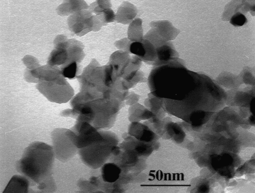
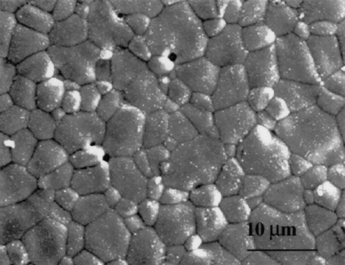
| Figure 1. (a) A TEM image of the as-received powders of yttria and (b) an SEM of a sintered and annealed sample of yttria. | |
 |
 |
| a | b |
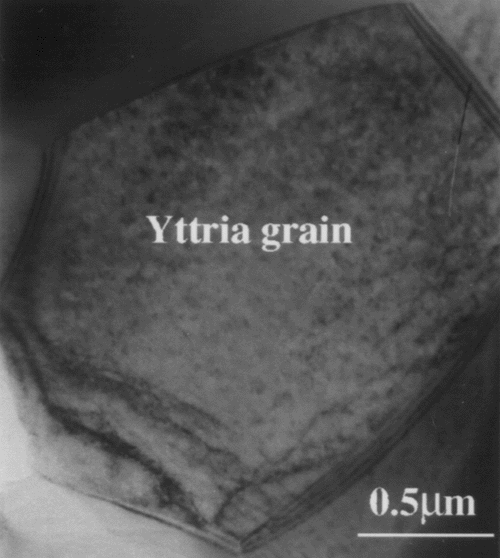
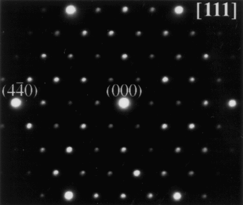
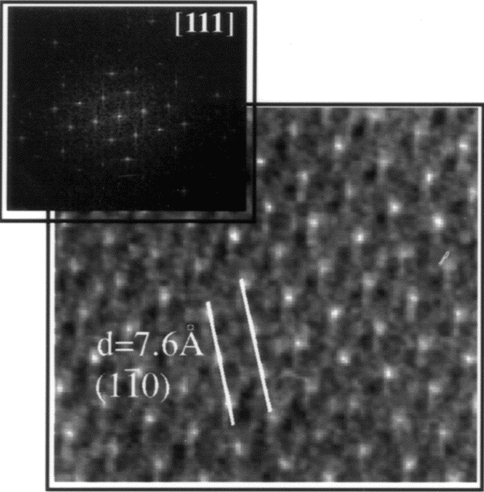
| Figure 2. (a) A TEM micrograph showing a faceted grain of a sintered yttria sample and (b) an SAD pattern of the [111]-type zone axis of yttria. Note the presence of extra reflections of the {110} and {330} type. | |
Optimization of the sensor behavior requires an understanding of the transport processes across the grain boundaries of the sensing element and at electrode interfaces, controlling doping effects, and evaluating the performance of packaging materials.37
The starting material was a commercial powder of yttrium oxide. The morphology of the powder particles is shown in the transmission electron microscopy (TEM) micrograph of Figure 1a. Pellets were cold-pressed and subsequently sintered at 1,550°C for 24 hours in air, followed by aging at 1,100°C or different lengths of time.
Scanning electron microscopy (SEM) and image analysis were employed to obtain information on the grain growth and densification of the material during aging (Figure 1b). Single-phase grained structures were revealed by TEM analysis. A typical microstructure and selected area diffraction (SAD) pattern are presented in Figure 2. Microanalysis results did not reveal any impurity segregation at the grain boundaries of the tested samples. Aging did not induce significant structural or chemical changes. The electrical response of the material was found to be indifferent for various annealing times,41 indicating that sintering had already stabilized the electronic characteristics of yttria, and further densification and microstructural modification did not affect the bulk conductivity of the material. The extra spots seen in the SAD patterns (e.g., Figure 2b) along {110} and {330} directions would traditionally be attributed to double-diffraction effects.
For further analysis of the crystal structure of yttria, high-resolution electron microscopy (HREM) images were obtained of the sintered grains. Careful tilting and thin-crystal criteria considerations suggested that the extra spots are real structural effects that need to be further investigated. Figure 3 indicates how image processing of the obtained results supports the argument of extra reflections in the yttria's microstructure. Structural effects impact electronic properties, and thus, further analysis is currently underway to clarify this issue.
 |
 |
| a | b |
| Figure 3. (a) An HREM micrograph of yttria. The inset is the fast-fourier transform of the image corresponding to the diffraction pattern of the area of analysis. (b) A computer-processed image showing how the high-resolution micrograph would look if only allowed reflections had contributed to the image formation. | |
 |
|
| Figure 4. An SEM micrograph of the MgO system used to provide electrical insulation to a yttria-based thermistor tested in the CISM. The MgO grain boundaries appear to be free from any secondary phases, suggesting that the iron oxide impurities are dissolved in the matrix. | |
The electrical conduction of insulation materials was found to be greatly affected by impurity effects. Typical impurities found in the insulating systems studied at the CISM were silica and iron oxide. The latter was found to have a low resistance at high temperatures (e.g., only a few ohms at 1,000°C). This factor could significantly affect the electrical response of the insulation material (typically having a resistance of the order of M s) by, for example, causing short-circuiting effects when a continuous layer surrounding the matrix grains is formed, thus providing interconnected paths for electrical conduction.42 Therefore, a microstructural analysis was performed to assess the structural characteristics of the insulators prior to their electrical testing to study impurity segregation effects.
Figure 4 shows a typical backscattered electron imaging (BEI) micrograph of the MgO system containing 0.5 wt.% Fe2O3. No second phases could be detected at the SEM level. The grain contacts appeared to be clean, and there was a significant amount of remnant porosity. Sintering at 1,600°C could not produce a denser material, since the melting point of magnesium oxide is 2,800°C. Electrical tests performed between 900-1,250°C showed a significant decrease in the activation energy of the impurity-containing material (1.4 eV) as compared to pure MgO (2.5 eV).42 In summary, the microstructural analysis suggested that the impurity phase was dissolved in the MgO matrix. According to the incorporation reaction

the impurity phase acts as donor, thus reducing the resistance of the insulating phase at high temperatures.
 |
 |
 |
| a | b | c |
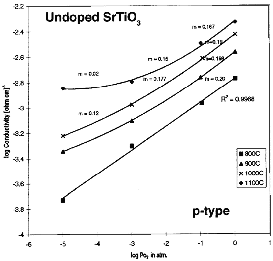
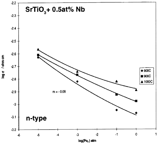
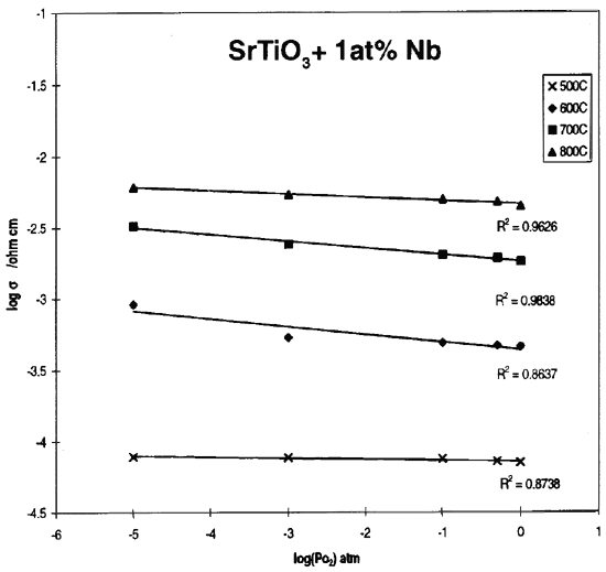
| Figure 5. Plots showing (a) the change in conductivity of the undoped SrTiO3 sample (having Sr/Ti = 0.98) showing the p-type behavior of the material at high temperatures. A minimum in conductivity is seen close to 10 ppm of oxygen. (b) Conductivity vs pO2 for the sample doped with 0.5 at.% niobium. The system was found to exhibit n-type behavior, but is still close to a minimum in conductivity. (c) Conductivity vs pO2 for the sample doped with 1 at.% niobium. The electrical behavior of the material becomes insensitive to pO2 changes at high temperatures. | ||
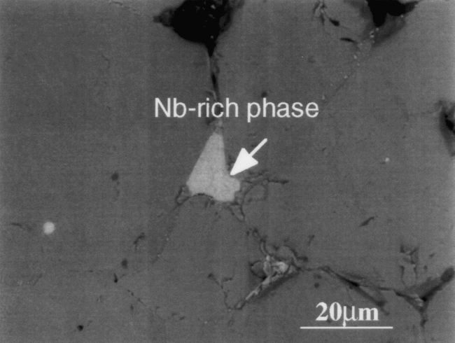
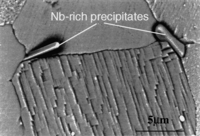
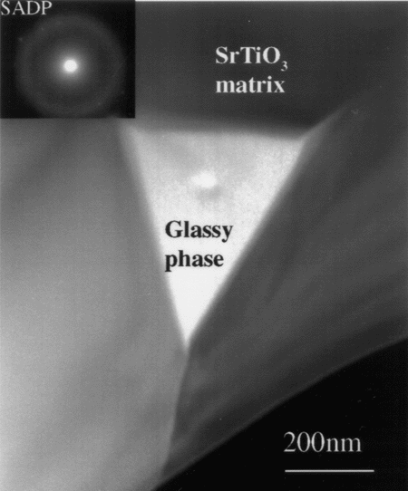
A microstructural examination of the SrTiO3-based system was then conducted to study the effects of niobium doping on the microstructure of the material. The material containing 0.5 at.% niobium was found to have small islands of niobium-rich and titanium-rich phases at grain junctions (Figure 6a). On the other hand, the 1 at.% niobium-doped system revealed the presence of niobium-rich precipitates at triple points, which controlled the grain growth of the material (Figure 6b). The most important finding, however, was associated with the presence of an amorphous phase at triple junctions in the sample doped with 1 at.% niobium (Figure 7). This phase was found to decompose in the microscope, as typically happens with the glassy phases formed in other electroceramic systems. Microanalysis showed that the amorphous component contained magnesium and aluminum (which are the major impurity species in the baseline material in concentrations on the order of 0.1 ppm level). The observed increase in the material's conductivity is likely to be associated with the presence of this amorphous phase, which acts as a sink for impurities.
 |
 |
| a | b |
| Figure 6. SEM micrographs of (a) the sample containing 0.5 at.% niobium, in which a niobium-rich phase is seen at the grain boundaries and (b) the sample containing 1 at.% niobium, in which niobium-rich precipitates formed at triple points were found to control the grain-growth process. | |
 |
 |
| a | b |
| Figure 7. (a) A DF TEM micrograph showing the presence of an amorphous phase at a triple junction of the SrTiO3 system containing 1 at.% niobium. The inset is an SAD pattern showing the ring pattern of this material. (b) The EDX analysis spectrum shows that the amorphous phase contains magnesium and aluminum impurities. | |
Traditionally, resistive gas sensors utilizing semiconducting oxides as sensing elements have been produced in the form of thick films.47 These are usually printed on Al2O3 substrates with electrodes attached to them.48 Thick films usually have thicknesses that range from about 10 µm to 100 µm or even more.49
Recently, there has been a trend toward developing planar sensors based on thin-film oxides with vapor-deposited catalytic activators. Thin films have enhanced compatibility with microfabrication techniques and lower power consumption. They can also be produced in arrays by including various chemically tuned elements to introduce a level of kinetic selectivity into the operation of each element.50 Thin films have thicknesses that range from a few angstroms to about 0.1 µm.49 In both thick- and thin-film sensors, the fundamental sensing process is the same (i.e., oxygen chemisorption and its reaction with the reducing gases).
Carbon monoxide sensors are essential to the control of emissions from combustion processes. The important parameters for a CO sensor are sensitivity, selectivity, and response time. Sensitivity is the percentage change in resistance when exposed to the reactive gas. Furthermore, for a sensor to be useful, it is necessary that it is selective to a particular gas with negligible cross-sensitivity to other gases. These parameters can be improved vastly by additions of various second-phase oxides and/or catalysts.51
TiO2-Based Thick Films
Rutile is the stable and most widely used form of titanium dioxide. Anatase is a metastable form of titania (TiO2) and transforms to rutile at temperatures that are dependent on factors such as grain size and impurities.52 Earlier work at the CISM showed that anatase-based systems could be used for gas-sensing applications at relatively high temperatures, provided that the anatase form is stabilized at the operating temperatures.53 Rare-earth oxide additions have been used for that purpose.54 Both anatase-yttria and anatase-lanthanum oxide systems have been successfully tested for CO sensing.53 Additions of palladium or CuO were shown to improve the sensing behavior of the systems tested.53,55
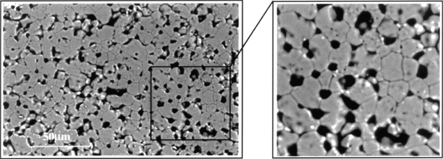
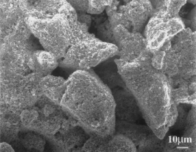
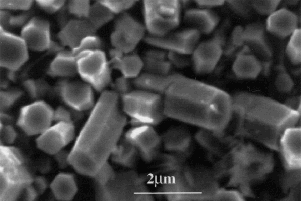
The anatase-based materials studied are complex systems having three components, each of which is expected to have a different effect on the physicochemical behavior of the material. The typical morphology of these systems is shown in Figure 8, which is a secondary mode scanning electron micrograph. The thickness of the thick films, as calculated from cross-sectional analysis of the samples, was commonly found to vary between 10-25 µm. The average surface porosity of a thick film (area fraction), calculated using image analysis, was found to be 25% (�3.0).
 |
 |
 |
 |
| Figure 8. An SEM micrograph showing a planar view of a thick film sensor. Note the formation of aggregates and the interconnected porosity in the sample. | a | b | c |
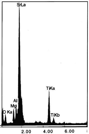
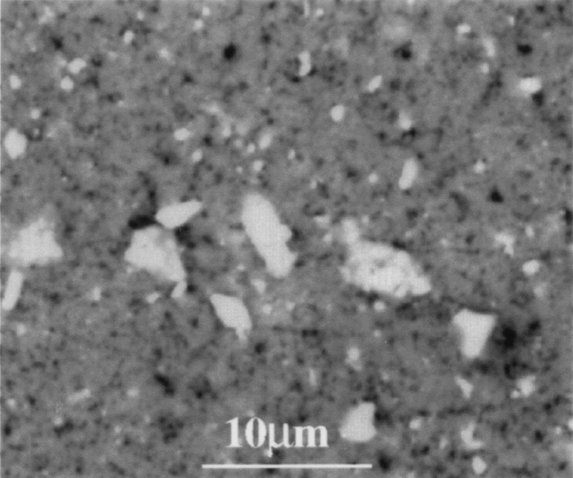
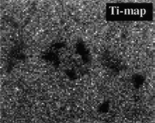
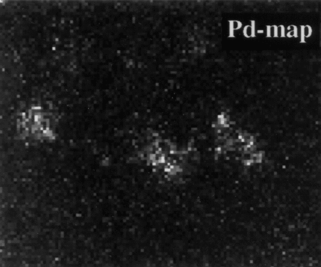
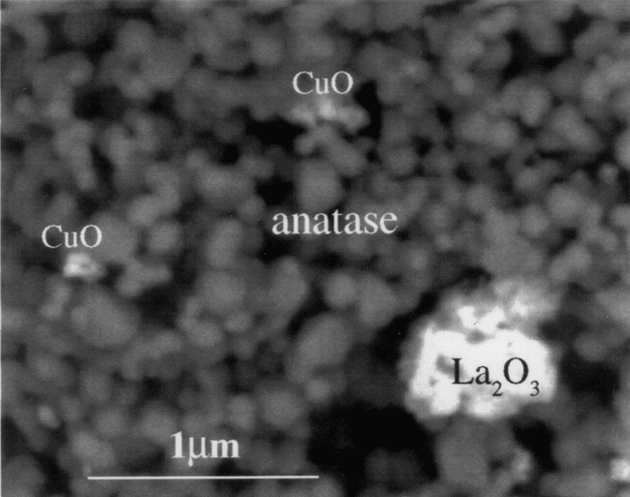
| Figure 9. A (a) BEI-SEM micrograph and (b) titanium and (c) palladium x-ray maps of the area showing the distribution of the various components using the elemental profiles. | |||
 0.5 µm long), and the smaller ones are clusters of very fine CuO particles on different sites in the TiO2 matrix.
 |
 |
 |
| Figure 10. A BEI-SEM micrograph showing the contrast of the various phases in a sensing system. The different phases can be distinguished with the help of EDX analysis, when there is no significance difference in their contrast. | a | b |
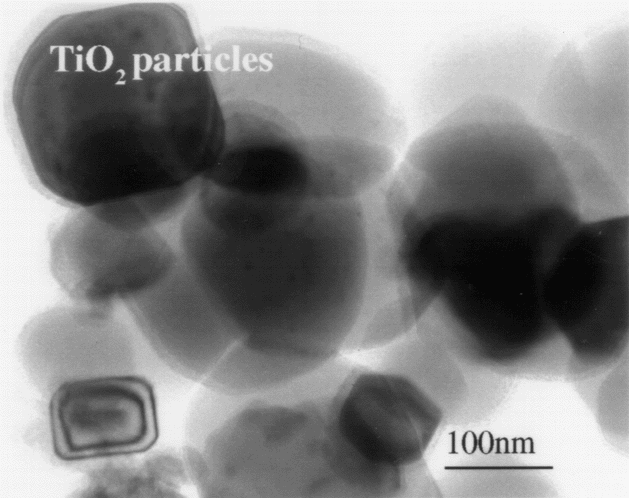
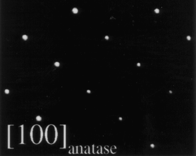
| Figure 11. (a) A TEM micrograph showing the TiO2 matrix particles of a thick-film gas sensor and (b) an SAD pattern of anatase. | ||
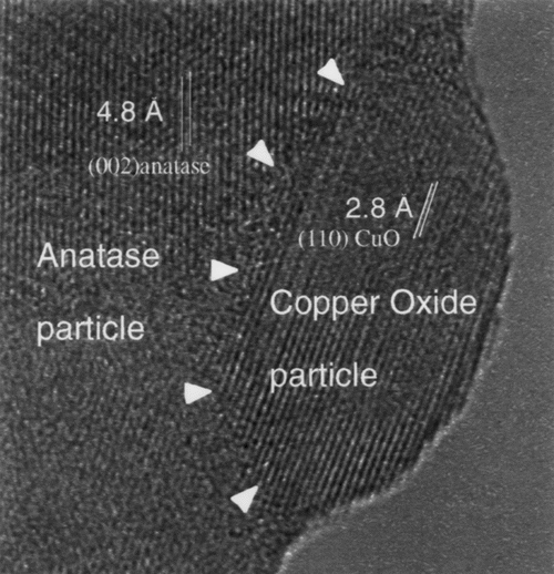 |
| Figure 12. An HREM of a thick-film gas sensor material, showing an anatase matrix grain having a very fine copper oxide particle attached to it. |
TiO2 Thin Films
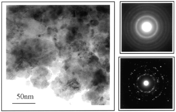
A sol-gel of titania was prepared according to the method described elsewhere.56 Drying the sol-gel of titania resulted in the formation of fine clusters of nanometer-sized particles having the anatase structure. An increase in the particle size was observed with time (from 3.5 nm to about 30 nm within an hour of TEM operation at 200 kV as determined by the electron diffraction patterns) (Figure 13). Thin films were deposited on sodium chloride substrates by spin coating. The films were found to consist of nanocrystalline more-or-less equiaxed grains (nanoparticles). The electron diffraction patterns showed rings corresponding to the anatase structure. The average grain size, as determined from the ring width, was about 8 nm. The film thickness was close to 1 µm, because multiple coatings were used to make sure that the film would cover the electrodes of the substrate for the sensing tests.
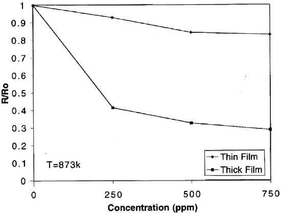
The thin films were tested at 600°C for CO sensing. The sensing behavior of the thin films is shown in Figure 14 and is compared with the electrical response of an anatase thick film tested under the same conditions. A microstructural analysis of the thin film after sensing showed that it consisted of overlapping layers (due to the multiple coatings) with granular structures and interconnected porosity (Figure 15). The films had the rutile structure, according to the diffraction information obtained. The morphology of the rutile particles tended toward the rod-like shape and toward plate-like shape, similar to the ones obtained from the transformation of commercial anatase particles to rutile, at high temperatures.57 The difference in the sensitivity between the thin and thick film thus appear to be related to the different crystal structures of the materials rather than the variation in the film's thickness alone. The thick film tested at 600°C had maintained the anatase structure; whereas, the thin film was fully converted to rutile at the same temperature. The anatase-to-rutile transformation in titania is a critical process that determines the sensor's sensitivity and selectivity.57,58 Further in-depth crystallographic analysis of the transition is currently underway.
 |
 |
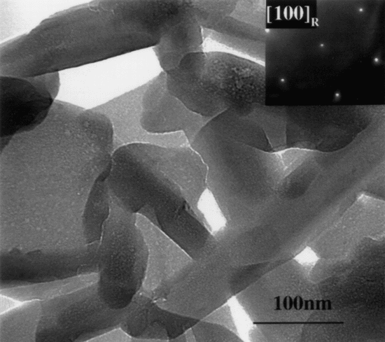 |
| Figure 13. A TEM micrograph of the sol-gel particles deposited on holey carbon grids. The insets are the SADs from the same area of the sample taken within one hour of the TEM operation at 200 kV. The grain size increased from 3.5 nm to 30 nm during that time. | Figure 14. A plot comparing the CO sensing behavior of an anatase thick film with that of a sol-gel thin film processed under the same conditions. The thin film sensor is shown to be less sensitive to the CO gas. | Figure 15. A TEM micrograph of a planar view of the thin film showing multiple layers and rod-like features; the crystal structure of its grains is rutile, as shown in the inset. Therefore, while the thick-film sensor consisted of anatase grains, the thin-film sensor had the rutile structure. The differences in the crystal structures, morphologies, and thicknesses of the materials of the two sensors result in varying sensing characteristics. |
The sensor configuration involves the open system with the bi-electrolyte: NASICON-yttria-stabilized zirconia (YSZ) and some auxiliary phases [e.g. NaNO3, Ba(NO3)2, Tb(NO3)3, etc.] for selective detection of NOx. NASICON and YSZ were attached to each other by diffusion bonding at 1,250°C. The potentiometric cell arrangement is
 |
|
| a | |
 |
 |
| b | c |
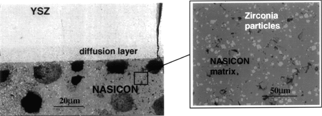
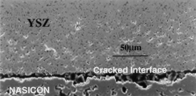
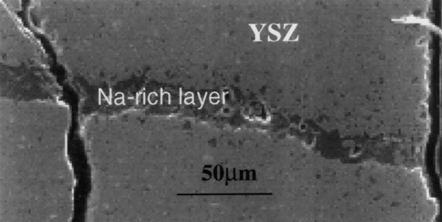
| Figure 16. BEI SEM micrographs showing cross-sectional views of the NOx sensor, including (a) the intact NASICON-YSZ interface, where the NASICON side contains zirconia precipitates; (b) the cracked NASICON-YSZ interface; and (c) sodium contained within the cracked channels of the YSZ side of the sensor. | |
Figure 16 shows several cross-sectional views of the sensor components. The NASICON side of the sensor was very porous and contained numerous homogeneous distributed precipitates60 that are rich in zirconium. Analysis revealed that these are zirconia particles. Earlier studies have suggested that its presence has a negligible effect on ionic conductivity.61 Furthermore, the interface between NASICON and YSZ was poorly bonded. Thus, the diffusion process used to bind the two materials together was not efficient. A porous 100 µm long interdiffusion layer was also seen within YSZ, near the interface. The YSZ part of the sensor was found to contain sodium in its pores and along cracked paths. The sensor material-platinum electrode contacts were also found to be cracked, and the contact regions were dissociated. These microstructural damages are believed to be primarily responsible for the poor performance of the sensor.
Figure 17 illustrates some characteristic microstructures of the iridium-oxide films. In order to reduce the drift in the pH sensitivity, the oxide film must be very dense and uniform (Figure 17a). Impurity (e.g. sodium, chlorine, or aluminum) effects, on the other hand, were found to degrade the electrode's performance. The impurities were shown to change the crystal structure of the material (e.g., Figure 17b). Microstructural evaluation guided the optimization of the film fabrication process, and a high-performance pH electrode was obtained.
 |
 |
| a | a |
| Figure 17. SEM micrographs showing (a) a planar view of a dense and thick iridium oxide film on an iridium wire that made an electrode with good performance and (b) a planar view of another iridium oxide film containing impurities. The presence of impurities has resulted in the modification of the crystal structure of the material. Notice the hexagonal crystals forming out of the iridium wire (pure iridium oxide typically has a tetragonal structure). | |
The second technique, known as electron holography, requires a field-emission-gun-based high-resolution TEM and a biprism.65 This method allows for space charge measurements at the grain boundaries of electroceramic materials66,67 and three-dimensional structural studies of nanocrystalline materials,68 such as catalysts. This technique could nicely complement high-resolution TEM analysis currently performed routinely for ceramic materials.
| CISM-BASED SENSOR RESEARCH |
|---|
|
Dedicated to the R&D of advanced sensing devices, ranging from thermistors to gas sensors and biosensors, the CISM is a multidisciplinary organization jointly funded by the National Science Foundation, Ohio, and an industrial consortium. Most of the sensor components studied are made of electronic ceramic materials, and a significant amount of research is focused on (oxide) semiconducting resistive sensors (for which the sensing characteristics rely on the resistance changes of the material, with changes in the physical property or chemical substance detected36).
Figure A shows the interaction between the various focus groups at the CISM. Communication of each group's results to other relevant groups is achieved by attending regular meetings and workshops. In this way, an integrated effort is underway to optimize the processing/microstructure/sensing property relationship of a particular sensor. Several model systems are under development for different applications, namely, high-temperature thermistor materials, gas sensors, and sensor component materials. The microstructural characteristics of these systems have been studied by means of electron microscopy techniques, such as scanning electron microscopy, conventional transmission electron microscopy, high-resolution electron microscopy, and microprobe analysis. Computer simulations and image processing were used to complement the characterization of the materials. All of the materials examined have been processed and tested within the CISM. The correlation of the microstructural evolution during processing/sensing and the mechanisms responsible for the materials response to different stimuli were reviewed. 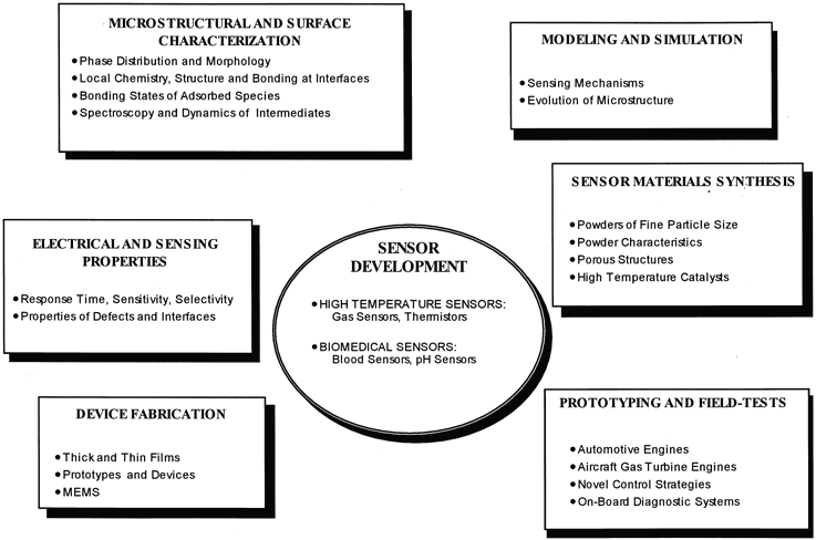 Figure A. The organizational structure of the NSF Center for Industrial Sensors and Measurements, showing the interactions among its various groups. |
ABOUT THE AUTHORS
P.I. Gouma earned her Ph.D. in materials science and engineering at the University of Birmingham in 1996. She is currently a postdoctoral research associate at Ohio State University. Dr. Gouma is a member of TMS.
S.A. Akbar earned his Ph.D. in materials engineering at Purdue University in 1985. He is currently director of the National Science Foundation's Center for Industrial Sensors and Measurement at Ohio State University.
M.J. Mills earned his Ph.D. at Stanford University in materials science and engineering in 1985. He is currently an associate professor at Ohio State University. Dr. Mills is a member of TMS.
For more information, contact P.I. Gouma, NSF Center for Industrial Sensor and Measurements, 477 Watts Hall, 2041 College Road, Columbus, Ohio 43210; (614) 292-7427; fax (614) 688-4949.
Direct questions about this or any other JOM page to jom@tms.org.
| Search | TMS Document Center | Subscriptions | Other Hypertext Articles | JOM | TMS OnLine |
|---|