 |
51 (3) (1999), pp. 22-27. |
|---|
|
51 (3) (1999), pp. 22-27. |
|---|
 |
| TABLE OF CONTENTS |
|---|
 dielectric, the effect of decreasing pitch and feature size on the package interconnects, the development and implementation of organic substrates, and advanced underfills for fine-pitch flip-chip applications. From a materials reliability aspect, important materials issues include enhanced solder interconnect reliability,
  -particle-induced soft errors, and the introduction of lead-free solder alloys.
In the past, advances in silicon semiconductors had little or no effect on the electronic-package design or process. New advances in silicon devices have driven increases in chip speed, device density (e.g., the number of transistors/mm2), and power dissipation. These changes, and those planned in the future, require larger numbers of interconnects to and from the devices, improved electrical performance, more effective thermal management, software systems to design and model the assembly, and different sets of materials to make these changes happen. Furthermore, the package is shrinking to a minimalist version of the products that traditionally have been called packaging. The chip and board have become a conjugate packaging system that must provide the traditional levels of electrical, mechanical, thermal interfaces, and environmental protection, with the additional challenge of increased performance.1 In addition, the boundary between where the device ends and where the package begins has become blurred with passive devices (e.g., resistors, capacitors, etc.) in the package and redistribution layers that act as space transformers on the chip. Electronic packaging is becoming one of the greatest challenges in manufac-turability, performance, and reliability in advanced electronics applications.
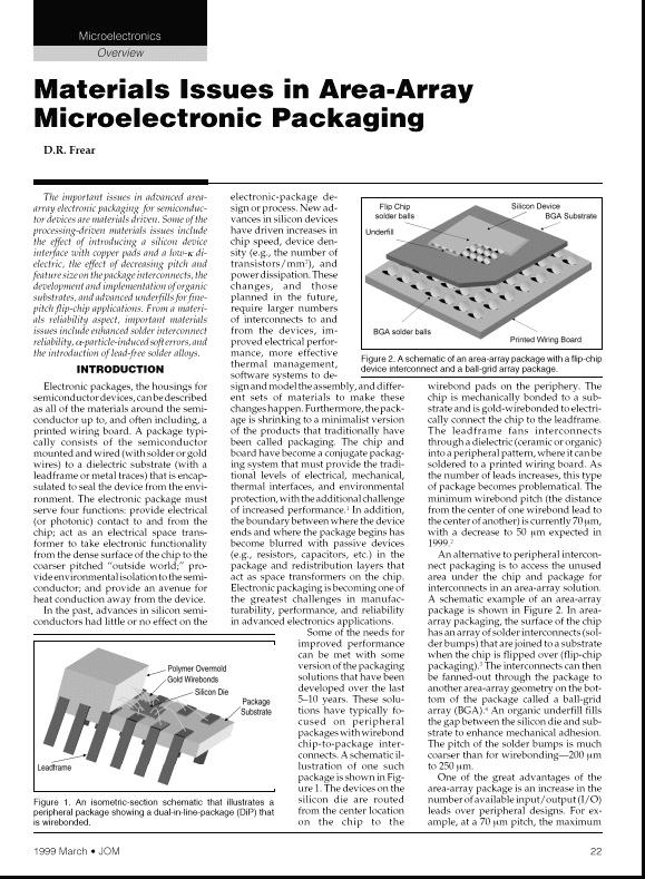
Some of the needs for improved performance can be met with some version of the packaging solutions that have been developed over the last 5-10 years. These solutions have typically focused on peripheral packages with wirebond chip-to-package interconnects. A schematic illustration of one such package is shown in Figure 1. The devices on the silicon die are routed from the center location on the chip to the wirebond pads on the periphery. The chip is mechanically bonded to a substrate and is gold-wirebonded to electrically connect the chip to the leadframe. The leadframe fans interconnects through a dielectric (ceramic or organic) into a peripheral pattern, where it can be soldered to a printed wiring board. As the number of leads increases, this type of package becomes problematical. The minimum wirebond pitch (the distance from the center of one wirebond lead to the center of another) is currently 70 mm, with a decrease to 50 mm expected in 1999.2
 |
| Figure 1. An isometric-section schematic that illustrates a peripheral package showing a dual-in-line-package (DiP) that is wirebonded. |
One of the great advantages of the area-array package is an increase in the number of available input/output (I/O) leads over peripheral designs. For example, at a 70 µm pitch, the maximum number of wirebonds on a 10 mm chip is less than 600. For an area-array package on the same 10 mm chip, even at the coarser bump pitch of 250 µm, the number of available I/O interconnects increases to 1,600.
Furthermore, it is difficult to design the sweep of wires from the chip to the leadframe in peripheral packaging to eliminate shorts and minimize inductance between adjacent wires. These issues are not present in the much coarser pitched area-array package. In a flip-chip package, the solder interconnects can also act as heat sinks because they are attached to the active surface of the silicon and are massive enough to draw heat away from the silicon.
 |
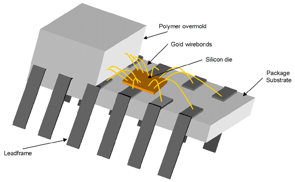
| Figure 2. A schematic of an area-array package with a flip-chip device interconnect and a ball-grid array package. |
The requirements for improvements in the functionality of electronic devices will also drive an area-array package solution. High-performance applications have an I/O range of 1,000-2,000 with a voltage drop power requirement and ground availability in the middle of the chip, rather than at the edges, which results in a drive toward a flip-chip area-array solution. Hand-held (e.g., cellular telephones) and cost-performance (e.g., desktop and portable computers) applications have a lower I/O requirement, with a form factor that requires a tighter density of I/Os provided by an area-array package.
Even with the advantages created by area-array packaging, performance, reliability, and cost requirements are challenging currently available area-array electronic package design. The majority of these challenges are materials driven.
 |
| Figure 3. The assembly and packaging challenge. (Derived from the The National Technology Roadmap for Semiconductors Technology, 1997 edition, published by SIA).2 |
The flip-chip solder interconnects are typically a high-lead-content solder alloy (e.g., Pb-5Sn or Sn-3.5Pb, in wt.%) that has a melting point in excess of 300°C. This high-melting-temperature solder alloy does not reflow during subsequent soldering processes (e.g., substrate to board reflow). The solder is reflowed to form solder balls, and the wafer is then diced. For assembly into a package, the silicon die is soldered to a ceramic, or organic, substrate. A silica-filled anhydride resin underfill is then flowed and cured under the die to enhance mechanical adhesion. The substrate is patterned to mirror the configuration of the solder balls on the die. The substrate pads are metallized to be wettable by the solder. The substrate acts to redistribute the leads to a coarser pitch on the BGA side.
To form the BGA interconnects, solder balls are mechanically placed on the substrate lands using mechanical fixtures. The solder alloy for the BGA interconnects is typically a near eutectic Sn-Pb alloy that melts at 183°C. The balls are fluxed and reflowed to join to the substrate. Welding, or brazing, or glass sealing a lid on the die or by flowing and curing an organic encapsulent (glob top) over the die completes the package. The package is then ready for assembly to a printed wiring board.
| Table I. Materials Used in Electronic Packaging | |
|---|---|
| Material | Application |
| Semiconductors | Si, GaAs |
| Metals | Solders for interconnects (Sn-Pb, Sn-Ag; gold wirebonds; copper leadframes (Kovar, CuBe, Alloy 42); copper traces in substrates; tungsten, molybdenum traces in co-fired ceramics; Ag, Au, Pd for thin/thick films on ceramics; and nickel diffusion barrier metallizations. |
| Ceramics | Al2O3 substrates modified with BaO, SiO2, CuO,etc.; SiN dielectrics; diamond heat sinks. |
| Polymers | Epoxies (overmold); filled epoxies (overmold); silica-filled anhydride resin (underfills); conductive adhesives (die bonding, interconnects); laminated epoxy/glass substrates; polyimide dielectric; benzoyclobutene; silicones; and photosensitive polymers for photomasks. |
| Glasses | SiO2 fibers for optoelectronics; silicate glasses for sealing; borosilicate glass substrates; and glass fibers for epoxy/glass substrates (F4-4). |
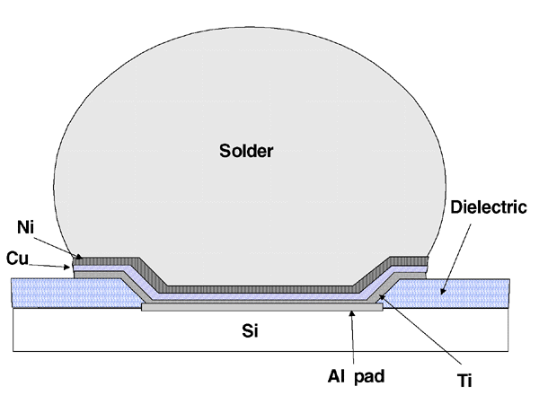 |
| Figure 4. A cross-section schematic of a UBM and solder bump for a flip-chip interconnect. |
 Dielectric dielectrics with < 3) provide a reduced capacitance and cross-talk between conductors. The low- material is used as a dielectric insulator in the interlevel dielectric (wiring the silicon out to the first package interconnect) with a matrix of copper or aluminum interlaced, typically using a dual damascene process.5-7 An example of a low- material being considered for semiconductor devices is the photosensitive benzocyclobutenes (photo-BCB) polymer8 that has a = 2.65. The damascene process and resultant one-layer metal structure is shown in Figure 5.
The devices for which copper and low- dielectric are the most suitable also require area-array packaging, involving flip-chip interconnects, in order to accommodate the large number of I/Os expected with these devices. The flip-chip array also reduces cross talk that could occur in wirebonded packages, because the long wires can act as antennas and create an inductive current in nearby conductors.
The move toward the use of copper and low on the die could potentially affect the manufacturability and reliability of the packaged devices. The significant issues involved in packaging copper and low k involve bonding with the copper and structural stability of the dielectric during processing and in service. Many of the currently used low- materials have properties that degrade at processing temperatures in excess of 250°C due to extensive cross-linking in the polymer. Therefore, the solders that must be used to interconnect with the copper/low- silicon device must have a suitable process temperature. The solder alloy proposed for this application is the near eutectic Sn-Pb alloy that melts at 183°C.
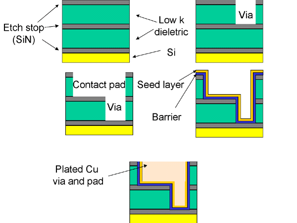 |
| Figure 5. Process steps to fabricate a dual damascene structure with copper and a low- dielectric. (Adapted from Hu and Harper.)7 SiN and low- dielectric deposition; via definition by etch; pad definition by etch; barrier (e.g., tantalum) seed (Cu) physical vapor deposition; and copper plating and chemical-mechanical polishing. |
These UBM structures were optimized for aluminum pad metallizations and may require changes for adhesion to copper pads. One metallization that has seen a great deal of development over the last few years and has shown a great deal of promise is electroless Ni-P. Electroless Ni-P has the advantage that it only plates over metal and, so, is a selective-metal-deposition technique as opposed to evaporation or sputtering, which require patterning and etching process steps. Electroless nickel has potential as a low-cost UBM and has a very slow reaction rate with tin. However, implementation of the electroless nickel as a UBM is not widespread because processing and reliability require further characterization efforts, but there are significant R&D efforts underway. Furthermore, electroless nickel is typically preceded by zincation on aluminum pads, which can not be performed on copper. A new process will need to be developed.
There are a number of materials and processing challenges associated with finer pitches. As the pitch shrinks, the methods to deposit the solder become more limited. Solder paste is very difficult to deposit using a silk-screen method at pitches below 150 µm due to rheological limitations of forcing a semi-solid (the paste) into small holes (the silk screen). Evaporation is difficult because developing a metal screen mask with the required tolerances is prohibitively expensive. Solder plating is still a good option, but the solder must be very uniform across each die. Solder ball uniformity is critical because large variations between die could result in electrical opens for small balls and shorts for large balls (Figure 6).
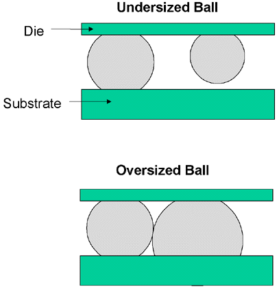 |
| Figure 6. The uniformity of ball size on the flip chip is important. (a) If the ball is undersized, electrical opens occur. (b) If the ball is oversized, electrical shorting is possible. |
The move to an organic substrate is the focus of an extensive development effort worldwide. The board interconnect density for flip-chip substrates must accommodate the increasing density of off-chip interconnect, and cost-effective substrate capability that combines the necessary fine line and micro-via features must be developed. Micro-vias are the metal-filled holes that provide a conduction path between copper lines in the multiple layers of an organic substrate. Micro-via capability must also scale with line width/spacing in order to provide the "via in-line" structures necessary to support bump-pitch densification. At current 250 µm pitches, micro-vias can be created using a photolithographic process. At finer pitches, laser-drilling techniques must be developed to create the required small via size.
Advanced substrates for flip chips must also provide increased wireability while delivering improved electrical performance with reliability levels at least equivalent to current surface-mount applications. New materials with dielectric constants approaching 2.0 and with coefficients of thermal expansion approaching 6.0 ppm/°C will be necessary to meet fine-pitch requirements. Furthermore, uniformity and flatness are critical for organic substrates to ensure uniform joint size and bonding across each die as the interconnect pitch decreases.
The change in substrate materials drives the need for a lower melting temperature solder to replace the high-lead-content Sn-Pb alloys that are processed in excess of 300°C for ceramic substrates. The organic materials in a substrate are typically epoxy-based and char or burn at temperatures in excess of 250°C. The most common solder alloy candidate is near-eutectic Sn-Pb that can be processed at 200°C. However, this could result in a situation where the flip-chip interconnect melts every time an additional solder reflow occurs during subsequent processing. Multiple reflows of the solder interconnects accelerates intermetallic growth between the tin of the solder and the metallized pads for the UBM and substrate. One way to circumvent this issue is to deposit low-melting-temperature eutectic Sn-Pb solder on the substrate lands or on the high-melting-temperature solder bump. Reflow to the substrate can be performed at eutectic Sn-Pb soldering temperatures, but the mixing between the high-lead-content and eutectic solder results in a higher melting temperature composition. Subsequent re-flows at eutectic Sn-Pb processing temperatures will not remelt the composite alloy flip-chip joint. This addresses the low-temperature processing requirements for organic substrates, but does not address the low- dielectric low-temperature processing requirements because the high-lead-content solder must still be reflowed on the silicon die.
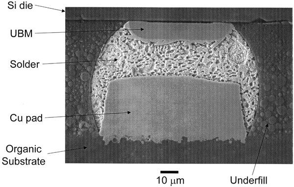 |
| Figure 7. An SEM micrograph of a flip-chip solder bump with silica-filled underfill. (Photograph courtesy of K.N. Tu at the University of California-Los Angeles.) |
Under thermal cycling conditions, the solder interconnects undergo microstructural evolution through heterogeneous coarsening and failure that results in electrical opens.9 This situation is alleviated, although not eliminated, through the use of the underfill for the flip-chip interconnects. Currently, BGA interconnects are not underfilled because they are much more massive and typically join materials with more closely matched coefficients of thermal expansion. As the pitch shrinks and the die size increases, the amount of strain imposed upon the solder interconnects also increases. The strain imposed on the solder joints follows the relation

 =
Ta/h
=
Ta/h
where is the shear strain imposed, is the difference in coefficient of expansion between the joined materials, T is the temperature change, a is the distance from the neutral expansion point of the joined materials, and h is the thickness of the interconnect.
An example of the change in strain follows: For the 250 µm pitch, a die of 17.3 mm2 has a = 8.65 mm and h = 110 µm; for 100 µm pitch, the die is 22.8 mm2 with a = 11.4 mm and h = 25 µm (numbers are taken from Reference 2). The temperature excursion is 100°C and the die is Si (6 X 10⁻⁶/°C) with an FR-4 substrate (17 X 10-6/°C). The resultant shear strains in the outermost solder interconnects at 250 µm and 100 µm pitch are eight percent and 50 percent, respectively. The larger strains result in more rapid fatigue failures in both the solder and potential fractures in the silicon if the underfill transfers the strain to the more brittle component.
This issue may need to be addressed with more compliant interconnects and underfill with more fatigue-resistant interconnects. Another potential solution is to use greater standoff solder interconnects with an aspect ratio much greater than one. This solution has been incorporated with great success on BGA interconnects using column grid arrays10 rather than standard balls.
The most significant emissions of alpha particles was from the lead in the solder interconnects. These radioactive sources are particularly insidious because the solder interconnects are located close to the silicon device and there are no barriers to absorb the particles. Lead and tin-lead alloys (solder) contain radioactive daughter elements of uranium and thorium that decay to form -particles. The principle cause of alpha emission is 210Pb (an unstable isotope found in lead) that decays by  - and -particles (-particle energy = 3.72 MeV) to form 210Bi (decays with - and -particles [3.72 MeV]) and then the very unstable isotope of 210Po, which subsequently decays with an -particle with an energy of up to 5.4 MeV.
As an example, a 5 MeV -particle penetrates into 25 µm of silicon and subsequently creates 1.4 X 10⁶ electron/hole pairs that can easily affect the charge state in a silicon device. The half life of 210Pb is 21 years, and 210Bi has a half life of 5.01 days. The half life of 210Po is 138.4 days, but there is a continuing accumulation of 210Po from the decay of the 210Pb. Commonly used lead for solders can have -activity as large as 1.0 /cm2-h.
Soft errors can become more predominant as gate size shrinks and the subsequent charge area in the silicon that results in memory decreases. Therefore, there is a need for a source of lead with a low -radiation rate to limit the possibility of soft errors. Some sources of lead ore have lower -radiation levels, but these are often contaminated during the smelting, handling, and processing steps. Low -Pb ore has an activity on the order of 0.02 /cm2-h.11 Since the half life of 210Po is 22 years, extremely old lead would not be expected to have a large -activity. For example, lead recovered from sunken Spanish galleons and old Roman ship anchors has an -activity of less than 0.001 /cm2-h.11 However, there is a very limited supply of this material. A newly proposed source (Pure Technologies) of low -Pb uses laser-isotope separation to refine lead to a state where -particle generation is drastically reduced to less than 0.0001 /cm2-h.11
It should be noted that cosmic radiation is also a source of alpha particles. At sea level, the cosmic radiation levels are on the order of 0.005 /cm2-h and dramatically increase with altitude. Cosmic radiation issues typically have been addressed through designs that increase the radiation hardness of the device. However, device engineers must be aware that it is difficult, if not impossible, to reduce the -radiation level below cosmic levels through materials changes.
-particle-induced soft errors. Therefore, efforts have commenced to develop lead-free solder alloys for area-array interconnects.
A number of tin-based solder alloys have been proposed as lead-free substitutes for packaging applications.13 There are no "drop-in" candidate alloys to replace eutectic Sn-Pb solder, but there are three alloys that stand out as strong possibilities for implementation as lead-free alternatives. These lead-free alloys, their melting behavior, and a brief discussion of their microstructure is given in Table II.
| Table II. Candidate Lead-Free Solder Alloys | |||
|---|---|---|---|
| Alloy | Liquidus/Solidus Temp. (°C) | Processing Temp. (°C) | Microstructure |
| Sn-3.5Ag | 221 (eutectic) | 20 | Tin matrix with precipitates of Ag3Sn |
| CuSbAgSn (Castin) | 211 (eutectic) | 240 | Tin-rich dendrites with lamellar Sn-Ag-Sb-Cu interdendritic regions |
| Sn-3.4Ag-4.8Bi | 201 (eutectic) | 230 | Tin-matrix surrounded by tin-rich and bismuth-rich lamella with Ag3Sn intermetallic precipitates |
From a mechanical properties perspective, these lead-free alloys exhibit a higher yield strength and slower creep deformation than eutectic Sn-Pb. However, the alloys are susceptible to interfacial delamination at the intermetallic/solder interface under tensile loading conditions.15 These lead-free alloys also have better fatigue performance than eutectic Sn-Pb, with the CastinTM alloy having the longest thermomechanical fatigue life.
In the past, the electronic package did not limit the performance of silicon devices. As the devices become faster and more powerful, the package can be the roadblock to desired functionality. Future device development must be a fully integrated approach between device design, device processing, and packaging to meet advanced performance requirements.
References
1. Electronic Materials Handbook: Volume 1: Electronic Packaging (Materials Park, OH: ASM, 1989).
2. The National Technology Roadmap for Semiconductors Technology (San Jose, CA: Semiconductor Industry Association, 1997).
3. L.S. Goldman, IBM J. Res. Dev., 13 (1969), p. 251.
4. J.H. Lau, IU (New York: McGraw-Hill, 1995).
5. K.J. Blackwell, I.I. Memis, and R.P. Kuracina, High Density Interconnect (HDI), 1 (4) (1998), p. 20.
6. P.C. Andricacos et al., IBM J. Res. Dev., 42 (1998), p. 567.
7. C.-K. Hu and J.M.E. Harper, Mater. Chem. Phys., 52 (1998), p. 5.
8. A.J.G. Strandjord et al., Int. J. Microcircuits and Electron. Packaging, 13 (1996), p. 360.
9. D.R. Frear, D. Grivas, and J.W. Morris, Jr., J. Electronic Materials, 17 (1988), p. 171.
10. T. Caulfield et al., Ball Grid Array Technology, ed. J.A. Lau (New York: McGraw-Hill, 1995), p. 131.
11. R. Brodzinski, "A White Paper on Alpha Activity in Lead" (Richland, WA: Battelle Northwest, 1998).
12. U S. Congress, Senate: Lead Exposure Reduction Act of 1994. DEC. 401 (1994).
13. NCMS Lead-Free Solder Project Final Report (Ann Arbor, MI: National Center for Manufacturing Sciences, 1997).
14. F.G. Yost, F.M. Hosking, and D.R. Frear, eds., The Mechanics of Solder Alloy Wetting and Spreading (New York: Van Nostrand Reinhold, 1993).
15. D.R. Frear and P.T. Vianco, Metall. Tran A, 25A (1994), p. 1509.
ABOUT THE AUTHOR
Darrel R. Frear earned his Ph.D. in materials science at the University of California at Berkeley in 1987. He is currently manager of the low-cost flip-chip project at Sematech. Dr. Frear is also a member of TMS.
For more information, contact D.R. Frear, Motorola, Semiconductor Product Systems, MD-EL725, 2100 East Elliot Road, Tempe, Arizona 85284; telehone (602) 413-6655; fax (602) 413-4511; e-mail r46897@email.sps.mot.com.
Direct questions about this or any other JOM page to jom@tms.org.
| Search | TMS Document Center | Subscriptions | Other Hypertext Articles | JOM | TMS OnLine |
|---|
 Dielectric