http://www.tms.org/pubs/journals/JOM/9908/Jackson/Jackson-9908.html
| |
http://www.tms.org/pubs/journals/JOM/9908/Jackson/Jackson-9908.html
| |
| TABLE OF CONTENTS |
|---|
Reductions in the computation time for models based at the atomic scale are needed because of the costs of supercomputer computing time, long turn-around times for models, complexity of input/output requirements, and non-user-friendly interfaces. Of these constraints, the turn-around time is of considerable interest because it constrains efforts at the process-modeling level for manufacturing engineering materials.
| ATOMIC-SCALE MODELING METHODS | ||||
|---|---|---|---|---|
| At the atomic scale, the immediate problem confronting any model is how to consider the interactions among the atoms, the number of atoms needed to model various effects, and how to view the output of the model. When dealing with atoms, the first inclination is to use quantum-mechanics methods, but the immediate problem arising here is what to use for the potentials in the Hamiltonian required by the Schroedinger equation (i.e., how the interactions among the atoms are represented). This question has been and continues to be studied in great detail. The bottom line of this approach is that very difficult computations must be accomplished that require very large machines. For real engineering materials, such as high-temperature superconductors, this approach is not practical in the context of process modeling.
A less demanding alternative is to use the molecular dynamics method.1 Here, equations for the motion of the atoms must be written, generating a set of simultaneous equations that must be solved for velocities and energies of motion and collision. This approach is very successful for organic-type molecules, although it still requires large machines for arrays of the molecules. Small arrays of a few tens of atoms or molecules can be handled on desktop machines rather nicely, but the software does not have process control or models built in, and the user interface assumes a working familiarity with molecular-dynamics details. A different approach to the problem is afforded by Monte Carlo methods, in which atomic behavior is viewed stochastically in terms of energies of various states and the transition probabilities among those states. The treatment of interactions can be viewed in terms of activation energies, energy wells, traps, and defects, which allows conceptual connections to be made easily to models of solids that are well established experimentally and theoretically. The advantage is that larger arrays of atoms, up to about 50,000, can be handled on desktop computers in reasonable times. The disadvantage is that the computational intensity is still high. The Monte-Carlo method requires energy computations at each time step in order to compute transition probabilities. Although considerably faster than quantum mechanical or molecular dynamics, the method is still not fast enough for real-time process modeling and simulation of film growth.
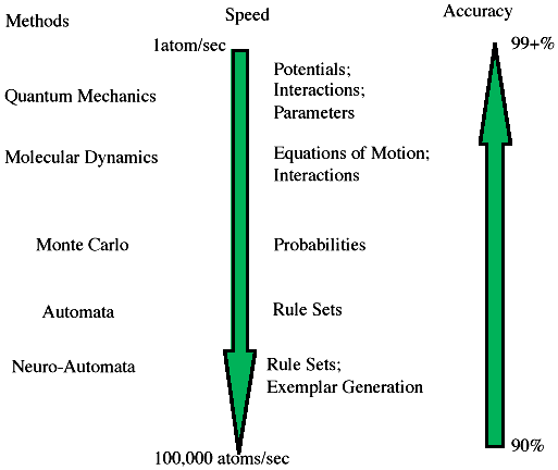
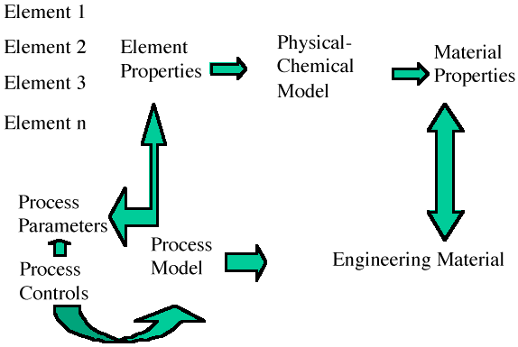
These time constraints on modeling impose severe operational difficulties on the methods used. To produce a working model of film growth that allows a user to stop the process, modify a parameter, restart the process, and record the model for future reference means that the computational scheme must be suited to high-speed computation and output display in a form the user can easily understand. As suggested in Figure A, the trade-off required for higher speed methods is prediction accuracy. However, such a reduction in accuracy is not entirely bad. If, by using these methods, one can obtain good estimates of parameters or behavior, particularly for a complex process, then more accurate methods can be applied to this grosser model to enhance the accuracy. The result is a considerable time savings to obtain a material design or process enhancement. In addition to these accuracy trade-offs, modeling of the film and the process for growing the film must be integrated into a seamless model (Figure B). This calls for designing the model to include both the physical/chemical behavior and the process-control parameters needed. At the atomic scale, models must be able to handle the discrete nature of the interactions among atoms, molecules, and other species whose size is about the same as the objects of which they are composed. The Monte Carlo method does this by using transition probabilities associated with each configuration of atoms, and molecular dynamics uses the separations between atoms or molecules based on some potential assumed to be valid. Each method in effect tracks each atom during the computation. When the number of atoms is less than a few tens of thousands, such detailed tracking is reasonable, but as the number of atoms increases beyond this, the time for computation increases accordingly. Ways to avoid this are used—nearest and next-nearest neighbor interactions may be used to limit the immediate number of atoms required in the calculation, but both Monte Carlo and molecular dynamics still require calculation over all the atoms for each step. |
This article focuses on discrete modeling in the microsecond to millisecond time ranges and on the subnanometer to micrometer spatial scales. These ranges are of immediate interest for film formation for optical, semiconductor, or ceramic-type films.
The most well know discrete model is the Ising model, in which the objects have only two states, usually represented as 0 and 1 or –1/2 and +1/2. Its application to magnet systems is well explored in the literature. A generalization of the Ising model is the Potts model, in which the states can assume more than two values. In either case, one must evaluate the state of the system at each step to determine what the state will be at the next step.
In this article, implementation of this method is to consider only the immediate neighborhood of atoms or objects and determine the possible actions an atom could take based on the occupants of its neighborhood (i.e., a set of rules is formulated based on expected interactions between small groups of atoms). Whether or not a rule is applied is determined via an activation energy that is applied in an Arrhenius-like function to find the probability of the rule being valid. This is essentially the Metropolis algorithm modified for the model. Since there are many possible rules, a probability partition diagram is created, to which the Metropolis algorithm is applied. The output is a state for the atom. Once this has been determined, a diffusion algorithm is applied to determine if the atom moves to a new location or remains at its present position.
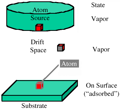
Figure 1 is a schematic of the space used in the model. A source of atoms provides atoms that drift to the surface using a drift vector combined with a random walk. This insures that no site is accidentally preferred by any atom from the source. The state is vapor until the atom reaches a surface atom, at which time the state becomes adsorbed.
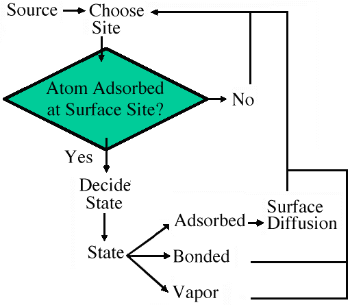
At the surface, the state algorithm fires and the atom may be placed in one of four possible states: remain vapor, bond to a like atom, bond to an unlike atom, or remain adsorbed, in which case the atom is available to surface diffuse to an open site nearby (Figure 2).
Although this concept is simple, application is somewhat difficult. There are several issues with neural nets that complicate their use. First, the exemplars used (the examples of inputs and outputs) must be a fair sample of the possible behaviors inherent in the model. Second, the necessary inputs and outputs must be carefully explored to identify the best combination of and the smallest number of inputs.
Once this has been accomplished, the real-time additional computation burden is minimal; in fact, rates as high as 200,000 atoms/s are feasible. Off-line training time, however, may still be long (hours). Still, the ability to model atomic behavior using this neurocomputing approach provides at least five orders of magnitude improvement in computation time. Desktop computing and the display of atomic modeling of thin films is possible and economical relative to hardware costs and user time.
 |
 |
| Figure 1. A schematic of a physical model. | Figure 2. The order of decisions used in generating the state and coordinates of atoms in the model. |
Alternatively, consider the scales involved and the phenomena associated with each scale. As the scale changes from a few nanometers to a few hundred, the objects of interest change from the atoms themselves to collections of atoms in the form of islands or grains with or without various types of defects. In the range from a few hundred nanometers to a few micrometers, the objects become the collections of grains and their distribution (the microstructure), and these collections have properties of interest, such as boundary sizes, orientations, defects, and phases. At larger scales, the geometry becomes important as this subsumes the microstructure as a focus.
The discrete models transition from the atomic to larger scales by shifting the focus to collections of atoms and the properties of the collections. The cellular automata-neurocomputing approach is designed to accomplish this transition by defining the algorithms in terms of objects whose associated features change with the scale involved.
 |
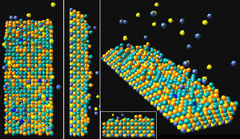 |
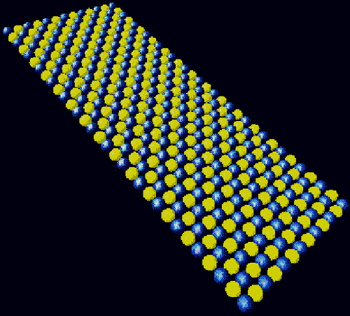
| Figure 3. The bare substrate used for testing the model simulation. | Figure 4. Views of the simulated film. |
Once a set of exemplars is available and the net is trained and tested, a matrix file is generated that is representative of the network and contains the atom interactions. The computation engine reads this net, and the simulation is ready to proceed.
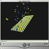
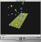
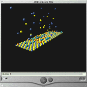
Simulation results for a 30 second simulation time are shown in Figure 4. The actual time to generate this image was 30 seconds live time. The simulation can be stopped and conditions changed at any time during the run. Video clips of examples of film growth are presented in Figure 5.
 |
 |
 |
| a | b | c |
Reference
1. J.M. Haile, Molecular Dynamics Simulation (New York: John Wiley & Sons, 1992).
ABOUT THE AUTHORS
A.G. Jackson and M.D. Benedict are with the AvXm Partnership, supported under contract with Materials Directorate at Wright-Patterson Air Force Base.
For more information, contact A.G. Jackson, AvXm Partnership, 5375 Oakvista Place, Dayton, Ohio 45440-2634; telephone (937) 436-3531; fax (937) 438-8026; e-mail Allen.Jackson@avxm.com.
Direct questions about this or any other JOM page to jom@tms.org.
| Search | TMS Document Center | Subscriptions | Other Hypertext Articles | JOM | TMS OnLine |
|---|