 Presenting a Web-Enhanced Presenting a Web-Enhanced Article from JOM |
 LATEST ISSUE |
|||
TMS QUICK LINKS: |
• TECHNICAL QUESTIONS • NEWS ROOM • ABOUT TMS • SITE MAP • CONTACT US |
JOM QUICK LINKS: |
• COVER GALLERY • CLASSIFIED ADS • SUBJECT INDEXES • AUTHORS KIT • ADVERTISE |
|
| Magnetic Materials and Devices | Vol. 63, No.10 pp. 25-28 |
Films Doped with Non-Magnetic
Transition Metals
Paul Slusser, Dhananjay Kumar, and Ashutosh Tiwari
Questions? Contact jom@tms.org. |
|
This paper presents the magnetic behavior of CeO2-δ films doped with two non-magnetic transition metal elements: copper and zinc. High quality films were grown on LaAlO3 (001) substrate using a pulsed laser deposition technique. Detailed structural characterization and magnetic property measurements were performed. Our results showed that Cu-doped CeO2-δ films exhibit room temperature ferromagnetism while Zn-doped CeO2-δ films are non-magnetic.
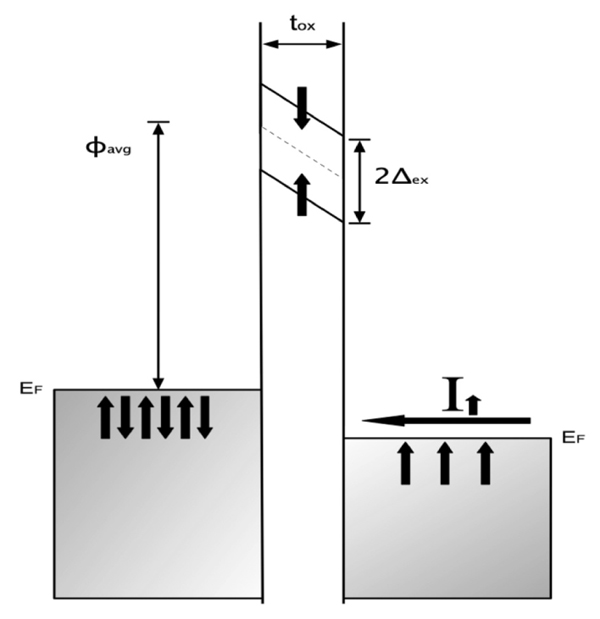
In the field of semiconductor electronics the progress over the past halfcentury cannot be overstated. Since the invention of the transistor in 1947, there has been unprecedented scientific and industrial progress in this field. Miniaturization is one of the most amazing aspects of this progress because it yields better performance at reduced cost and reduced power consumption. However, the miniaturization of electronic and magnetic devices is becoming increasingly challenging because the physical properties of the materials have become the limiting factors in device fabrication. These difficulties and challenges stem from the operational physics of these devices. When the gate length of transistors decreases, the probability of electron tunneling increases. Thus, there are very real physical barriers to the scaling of complementary metal oxide semiconductor (CMOS) technology to the atomic level. The reality is that simply making the devices smaller can not be used as the primary method of performance improvement, and new methods will need to be developed. One of the possible new approaches to device design is based on the utilization of both the charge and spin degrees of freedom of electrons in device design. This area of research is broadly defined as spintronics.1–6 The operation of a spintronic device depends on the injection of spin-polarized carriers into the semiconductors. Presently, much research is under way to develop efficient spin injection materials. However, despite extensive efforts, efficient injection of spin polarized carriers into nonmagnetic semiconductors continues to be a major hurdle. Initial efforts to inject spin in semiconductors by using ferromagnetic metal electrodes in direct contact with semiconductors resulted in a very small (~1%) degree of spin polarization of injected carriers.7 For efficient spintronic devices, it is essential to achieve much higher spin injection efficiency. Some earlier studies showed that spin polarized carrier injection can be achieved by using a thin tunneling barrier layer (spin-filter) of a ferromagnetic dielectric between a nonmagnetic metallic electrode and the semiconductor.8,9 Figure 1 shows a schematic of a tunnel barrier. The barrier height Φavg at
temperatures above the transition temperature(TC) of the magnetic barrier
is shown by the dotted line. Below TC there is an exchange splitting (2Δex) of the conduction band leading to different barrier heights for the spin directions. The difference in barrier heights leads to a different transmission factor for each spin. Given the exponential dependence of the tunnel current on the
barrier height, a high degree of polarization can be achieved in this manner.
Equation 1 gives the tunneling current for a junction with an average barrier height of Φ following the method of Simmons.10 The model described in Equation 1 has been used by Moodera et al. to describe spin dependent tunneling in EuS.11 'Φ' is the average barrier height, 'S' is the barrier thickness, and 'm' is the effective mass of an electron in the conduction band of the contact material. J=J0(Φ-½eV)exp[-A(Φ-½eV½] (1) -J0(Φ+½eV)sxp[-A(Φ+½eV)½] (2) A={4πS/h}(2m)½ (3)
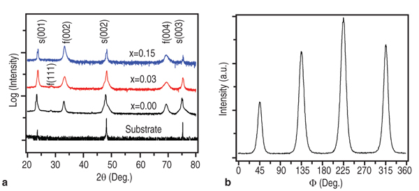
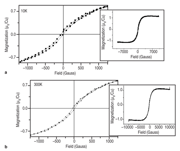
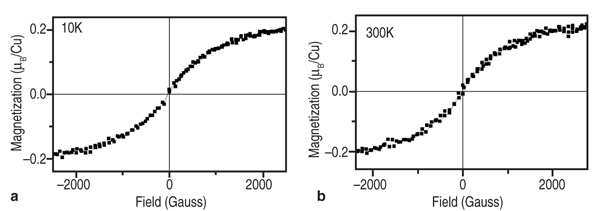
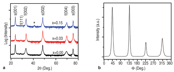
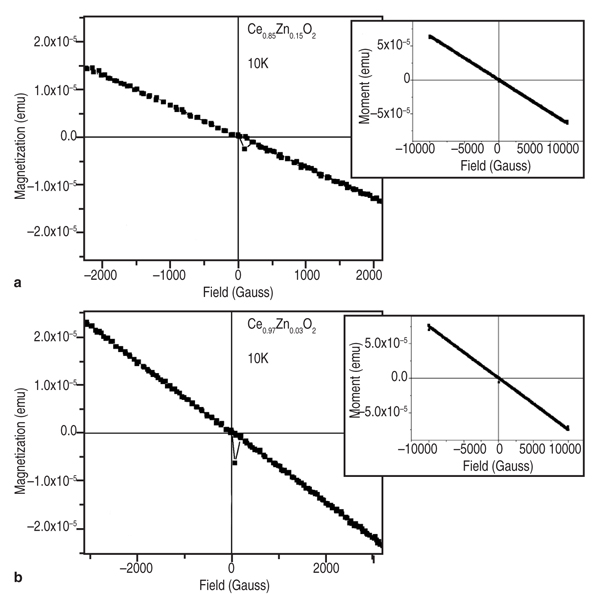
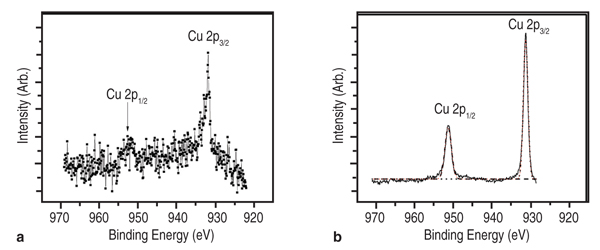
J0={e/2πh}S-2 (4)Equation 1 shows that for even slightly different barrier heights there is an exponentially large change in the current tunneled through the barrier. Thus even a small exchange splitting of the conduction band edge due to an internal magnetic field in the tunnel barrier can give rise to a highly spin polarized current. The extensive studies on the europium chalcogenides (EuX, X: O, S, Se) have demonstrated the feasibility of spin dependent tunneling through magnetically polarized barriers.12,13 However, europium chalcogenides exhibit Tc much lower than room temperature, rendering them useless for practical device applications. For real applications, spin filter material needs to be ferromagnetic at room temperature. In 2006, Tiwari et al.4 reported room temperature ferromagnetism in cobalt doped CeO2-δ. This work inspired dozens of other research groups to explore CeO2 system, and later on ferromagnetism was reported in Ni and Fe doped CeO2 also.14,15 Though the above inventions lead to much excitement in the materials science community, a significant debate continues about whether the observed properties are the intrinsic property of the material or an extrinsic property due to some kind of precipitates etc. The above controversy becomes still more severe because all the dopants tried with CeO2 thus far are magnetic in nature.4,14,15 If even a tiny fraction of these elements precipitates out, it can make the whole material appear to be magnetic. This paper reports a study of the magnetic behavior of Ce1-xCuxO2-δ and Ce1-xZn xO2-δ films grown on LaAlO3(001) substrates. The films were prepared by pulsed laser deposition and thoroughly characterized using state-of- the-art characterization techniques. X-ray diffraction patterns of the Ce1- xCuxO2-δ films grown on LaAlO3 (001)substrates are shown in Figure 2a. Diffraction patterns of the substrate are also shown. Major peaks belonging to the (00l) family of cubic cerium oxide were observed indicating the film is highly oriented in relation to the substrate. No secondary phases were observed in the films. Because the detection limit for x-ray diffraction (XRD) is around 1% this does not completely rule out secondary phases. θ-2θ XRD patterns for the films were collected on the Philips X'Pert system and Φ-angle diffraction patterns for the films were collected on the Bruker AXS system. Previous studies of cerium oxide grown on LaAIO3 using transmission electron microscopy showed that the films grew by domain matching epitaxy (DME).4 In this growth mechanism the [220] plane of CeO2 aligns parallel to the [020] plane of the LaAlO3 substrate. The c-axis of the substrate and the film are parallel in this growth mechanism, and there is a 45° rotation of the film relative to the substrate. Figure 2b shows the four-circle high-resolution x-ray Φ-scan for the Ce0.97Cu0.03O2 film for the (111) plane showing the cubic symmetry of the fluorite structure. The peaks spaced at 90° intervals reveal the cubic symmetry and a highly oriented film. Magnetic characterization of the films showed two different types of behavior. In the low concentration x=0.03 sample a ferromagnetic response was observed with a saturated magnetic moment of ~1 μB/Cu atom as shown in Figure 3a and b. As can be seen in the insets, the values of the saturated moments at 10 K and 300 K are almost similar indicating a Tc much higher than room temperature. The coercivity of the sample at 10 K was found to be ~70 Gauss and the remnant polarization was approximately 0.2 μB/Cu. A very different magnetic behavior was observed in the x=0.15 film as can be seen in Figure 4a and b. The saturated magnetic moment is approximately 0.2 μB/Cu atom. There is no observed coercivity for the x=0.15 film at any temperature, and the saturated moment is approximately 5 times lower than in the x=0.03 film. This type of behavior is symptomatic of a superparamagnetic response. To understand the observed magnetic behavior of the films, all possible electronic configurations of Cu ions in the material must be considered. Cu atoms in unionized state have an outer shell electronic configuration of 3d104s1, thus, Cu+ and Cu2+ ions are expected to have 3d10 and 3d9 configurations, respectively. In the 3d10 configuration, all of the d electrons are paired; therefore, a Cu+ ion does not have a magnetic moment. In the case of Cu2+ ions with a 3d9 configuration, one unpaired electron is available. This gives a spin angular momentum of ½ which can result in a net magnetic moment of M ~1.73 μB [M =gμB√(S(S + 1)); g = 2, S = 1/2].16 So an observed magnetic moment of 1 μB/Cu atom in the case of x=0.03 indicates that 68% of the copper ions in the film are in the 2+ state. On the other hand in the case of x=0.03 the observed magnetic moment of 0.2 μB/Cu atom indicates that 10% of the copper ions in the film are in the 2+ state. Figure 5a shows x-ray diffraction patterns of the Ce1xZnxO2δ samples. In the x=0 and x=0.03 scans, only reflections for the (001) family of Cubic CeO2δ and the LaAlO3 substrate were observed indicating highly oriented films. The x=0.15 film showed a minor peak belonging to a hexagonal ZnO (101) peak indicating that some degree of phase separation occurred in this film. A high-resolution four-circle phiscan XRD pattern is shown in Figure 5b for x=0 sample. The peaks spaced at 90° intervals show the cubic symmetry of the system. The results of the magnetic characterization for the zinc-doped films are shown in Figure 6. As can be seen in this figure a strictly diamagnetic response was observed in these films. This can be understood by the fact that the zinc ions were found to be in the 2+ state using x-ray photoelectron spectroscopy (XPS) and Zn2+ ions have no unpaired electrons and thus has no net magnetic moment. Investigating the valence state of the copper ions in the cerium oxide matrix is expected to give further insight to the origin of the films' magnetic properties. For this XPS experiments were performed. Figure 7a shows XPS data for the Ce0.97Cu0.03O2δ film for the Cu 2p lines. XPS peaks for the Cu 2p3/2 and 2p1/2 emissions were centered at about 933.0 eV and 953.4 eV, respectively, with an energy separation of 20.4 eV. In the case of elemental copper, peaks would be positioned at 932.6 eV and 951.0 eV with an energy spacing of 18.4.17 Since these energy values are very different from the experimentally observed values, the possibility of the presence of metallic precipitates in the films is ruled out. If the Cu exists in Cu1+ state, 2p3/2 and 2p1/2 peaks should be centered at 932.4 eV and 952.5 eV, with an energy separation of 20.1 eV.18 On the other hand in the case of Cu2+, photoelectron 2p3/2 and 2p1/2 peaks should occur at 933.5 eV and 953.7 eV, respectively, with an energy separation of 20.2 eV.18 The experimentally determined values of the binding energy and energy separation of Cu 2p photoelectron peaks in the x=0.03 film show that Cu ions are present in mixed valence state (Cu2+ and Cu+) with the majority of ions being in the 2+ state. The above finding is in very good agreement with the analysis of magnetic data. Figure 7b shows XPS data for the Ce0.85Cu0.15 O2 film. In this case the Cu 2p peaks are positioned at 951.5 eV and 931.5 eV with an energy separation of 20.0 eV. Similar analysis, as for the x=0.03 sample, shows that in x=0.15 films also Cu ions are again present in mixed valence state but this time the majority of them are in Cu+ state in good agreement with the analysis of magnetic data.18,19 An investigation of the magnetic properties of Cu and Zn doped CeO2 films found that both dopants are nonmagnetic in nature, but the doped films showed very different characteristics. Cu doped films exhibited ferromagnetic characteristics, while the Zn doped films showed diamagnetic behavior.
Paul Slusser and Ashutosh Tiwari are with the Department of Materials Science and Engineering, University of Utah, SLC, Utah 84112, USA; Dhananjay Kumar is with the Department of Mechanical Engineering, North Carolina A & T Greensboro, North Carolina. Dr. Tiwari can be reached at tiwari@eng.utah.edu. |
||