
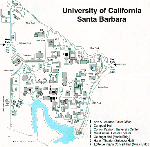
The technical sessions for the 1999 EMC will commence at 8:30 a.m., Wednesday, June 30, 1999. Sessions will be held on campus in the University Center, more detail is available by viewing a University Area Map. Topics for this year's meeting include growth and characterization of wide bandgap materials, quantum-effect materials, materials integration, organic optoelectronics and transistors, epitaxy, and in-situ and real-time characterization. A special topical session will be held on the role of defects in the properties of III-nitrides.
More detailed session information is available by downloading the Technical Program, presented in PDF format. The technical program will also be made available on-site to all paid registrants.
| TUESDAY, JUNE 29, 1999 | ||
|---|---|---|
| Registration | 3:00 p.m.-8:00 p.m. | University Center/Multicultural Lounge |
| WEDNESDAY, JUNE 30, 1999 | ||
| Registration | 7:30 p.m.-5:00 p.m. | University Center/Multicultural Lounge |
| Exhibit Booths | 10:00 a.m.-5:00 p.m. 7:00 p.m.-9:00 p.m. |
University Center/Multicultural Lounge |
| Welcome Reception | 7:00 p.m.-9:00 p.m. | University Center/Multicultural Lounge |
| Plenary Session: Dr. Shuji Nakamura (Including Student Awards Ceremony) |
8:30 a.m. | University Center/Corwin Pavilion |
| Session A. Semiconductor Quantum Dots–Devices | 10:00 a.m. | Multicultural Center Theatre |
| Session B. Materials Integration–Substrate Fabrication & Bonding | 10:00 a.m. | State Street Room |
| Session C. Characterization, Growth & Properties of Organic Electronic Materials | 10:00 a.m. | Santa Barbara Room |
| Session D. Oxides for Devices | 10:00 a.m. | Flying A Studios |
| Session E. Special Topical Session | 1:30 p.m. | Music Building--Lotte Lehman Hall |
| Session F. Semiconductor Quantum Dots-Formation & Structure | 1:30 p.m. | Multicultural Center Theatre |
| Session G. Epitaxy for Devices-B | 1:30 p.m. | State Street Room |
| Session H. Electronic Transport in Organic & Molecular Materials | 1:30 p.m. | Santa Barbara Room |
| Session I. Column IV Heterostructures & Devices | 1:30 p.m. | Flying A Studios |
| THURSDAY, JULY 1, 1999 | ||
| Registration | 7:30 p.m.-4:00 p.m. | University Center/Multicultural Lounge |
| Exhibit Booths | 10:00 a.m.-4:00 p.m. | University Center/Lagoon Plaza |
| Picnic: Evening at the Zoo | 6:00 p.m.-9:00 p.m. | Santa Barbara Zoological Gardens |
| Session J. Epitaxy for Devices-A | 8:20 a.m. | Corwin East |
| Session K. Nanoscale Characterization | 8:20 a.m. | Corwin West |
| Session L. Wide Bandgap AlGaN/GaN Heterostructures | 8:20 a.m. | Music Building--Lotte Lehman Hall |
| Session M. SiC Growth & Characterization | 8:20 a.m. | Multicultural Center Theatre |
| Session N. Infrared Materials & Devices | 8:20 a.m. | State Street Room |
| Session O. Issues for Ferroelectric & High Permittivity Thin Film Materials | 8:20 a.m. | Santa Barbara Room |
| Session P. Ordering in Semiconductor Alloys | 1:30 p.m. | Corwin East |
| Session Q. Nanostructure Self-Assembly | 1:30 p.m. | Corwin West |
| Session R. Properties of InGaN Heterostructures & Devices | 1:30 p.m. | Music Building--Lotte Lehman Hall |
| Session S. Silicon Carbide Processing for Devices | 1:30 p.m. | Multicultural Center Theatre |
| Session T. Materials Integration: Growth & Characterization | 1:30 p.m. | State Street Room |
| Session U. Thermophotovoltaic Materials & Devices | 1:30 p.m. | Santa Barbara Room |
| Session V. Thermoelectric & Other Narrow Gap Materials | 1:30 p.m. | Santa Barbara Room |
| FRIDAY, JULY 2, 1999 | ||
| Registration | 7:30 p.m.-10:00 a.m. | University Center/Multicultural Lounge |
| Session W. Epitaxy of III-V | 8:30 a.m. | Corwin East |
| Session X. Composite Materials & Applications | 8:20 a.m. | Corwin East |
| Session Y. Properties of Quantum Wires & Wells | 8:20 a.m. | Corwin West |
| Session Z. Wide Bandgap Nitrides (MBE, Theory & AlN) | 8:20 a.m. | Music Building--Lotte Lehman Hall |
| Session AA. Metal Contacts to Wide Band Gap Semiconductors | 8:20 a.m. | Multicultural Center Theatre |
| Session BB. Etching & Passivation of Compound Semiconductors | 8:20 a.m. | State Street Room |
| Session CC. Defects & Defect Engineering for Devices | 8:20 a.m. | Santa Barbara Room |
| Session DD. Non-Destructive Testing & "In-Situ" Monitoring/Control | 1:30 p.m. | Corwin East |
| Session EE. Semiconductor Quantum Dots-Electronic Structures | 1:30 p.m. | Corwin West |
| Session FF. Issues of Dopants & Defects in Nitrides | 1:30 p.m. | Music Building--Lotte Lehman Hall |
| Session GG. Epitaxy of II-VI & Chalcopyrites | 1:30 p.m. | State Street Room |
| Session HH. Epitaxy of Si, III-V, Oxides | 1:30 p.m. | Santa Barbara Room |
| Search | 1999 EMC Home | TMS Meetings Page | About TMS | TMS OnLine |
|---|