An Article from the January 2004 JOM: A Hypertext-Enhanced Article
|
TMS
ONLINE | TMS
PUBLICATIONS | SITE
MAP An Article from the January 2004 JOM: A Hypertext-Enhanced Article |
|
|
|
Debasis Bera is a Ph.D. student and Suresh C. Kuiry is a Research Associate in Advanced Materials Processing and Analysis Center and Mechanical Materials Aerospace Engineering Department, University of Central Florida (UCF). Sudipta Seal is an associate professor in Advanced Materials Processing and Analysis Center (AMPAC), Mechanical, Materials and Aerospace Engineering and Director for the Surface Engineering and Nanotechnology Facility. He is also the UCF Nanotechnology Initiative Coordinator. |
Exploring traditional, innovative, and revolutionary issues in the minerals,
metals, and materials fields.
|
| OUR LATEST ISSUE |
|
||
 |
||
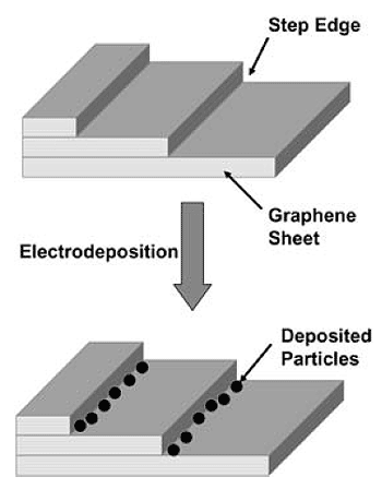
Figure 1. A schematic diagram for synthesis of naanoparticle arrays through active template-assisted synthesis. |
Overview: Nanoscale Surfaces
Synthesis of Nanostructured Materials Using Template-Assisted Electrodeposition |
Metals at the nanometer scale exhibit unusual behavior compared to their bulk counterparts. The manifestation of quantum phenomena in the electron transport of metallic nanowires is an example, as are the interesting magnetic properties of nanoparticles (transition metals) due to spin-polarized transport.1,2 Such unusual properties have generated interest in nanostructured materials for potential applications in biomedical sciences, electronics, optics, magnetism, and energy storage.3,4 These nanostructured materials can be synthesized by a number of techniques, such as inert gas condensation, plasma processing, physical and chemical vapor deposition, electrodeposition, mechanical alloying, rapid solidification, sol-gel, micro-emulsion, spark erosion, and severe plastic deformation.5 Although the use of many such techniques is limited to laboratory scale, inert gas condensation, mechanical alloying, and electrodeposition are among the methods that are available for commercial use. In this article, an overview of nanomaterials synthesis using electrodeposition techniques is presented.
The formation of nuclei on the electrode substrate was extensively studied on the basis of macroscopic thermodynamic considerations. The nucleation of nanostructures on the electrode substrate during electrodeposition is influenced by the crystal structure of the substrate, specific free surface energy, adhesion energy, lattice orientation of the electrode surface, and crystallographic lattice mismatch at the nucleus-substrate interface boundary.6,7 The final size distribution of the electrodeposits, however, strongly depends on the kinetics of the nucleation and growth. The electrodeposition process involves the formation of either an instantaneous or a progressive nucleation.8 In the case of instantaneous nucleation, all the nuclei form instantaneously on the electrode substrate, and subsequently grow with the time of electrodeposition. In contrast, the number of nuclei that are formed is a function of time of electrodeposition in the progressive nucleation. These nuclei gradually grow and overlap, and therefore, the progressive nucleation process exhibits zones of reduced nucleation rate around the growing stable nuclei. The electrodeposition method consists of an electrochemical cell and accessories for applying controlled current at a certain voltage. The cell usually contains a reference electrode, a specially designed cathode, and an anode or counter electrode. The cathode substrate on which electrodeposition of the nanostructure takes place can be made of either nonmetallic or metallic materials. Using the surface of the cathode as a template, various desired nanostructures or morphologies can be synthesized for specific applications. Such a template-assisted electrodeposition process can be broadly divided into two groups: active template-assisted and restrictive template-based electrodeposition.
Active Template-Assisted Electrodeposition
The formation of nanostructures in active template-based synthesis results from growth of the nuclei that invariably nucleate at the holes and defects of the electrode substrate. Subsequent growth of these nuclei at the template yields the desired surface morphology of the nanostructures, which can therefore be synthesized by choosing the appropriate surface of the electrode. Highly oriented pyrolitic graphite (HOPG), for example, is used extensively as an electrode substrate for the electrodeposition of silver,9–11 gold,12 molybdenum,13 palladium,14–16 and platinum17 nanostructures. Electrodeposition initiates at the step edges, dislocations, and defect sites of the electrode surface. Vázquez et al.9 studied the early stages of overpotential deposition of silver on HOPG from silver-ion-containing acidic solution. It was shown that the initial deposition occurred at the step edges of the electrode surface, and silver nuclei were not found on the flat HOPG surface domains. The electrodeposition study10 of silver on the HOPG substrate using in-situ scanning tunneling microscopy revealed that at low over-potentials, the deposition process on the atomically flat terraces of HOPG was inhibited because of weak substrate-deposit interaction leading to preferential silver deposition at step edges and other surface defects. Such step-edge deposition involves the preferential nucleation and subsequent growth of nanoparticles on a certain crystal surface. Figure 1 shows a schematic diagram of step-edge synthesis. Favier et al.16 attempted to fabricate hydrogen sensors and switches with the help of palladium nanoparticles electrodeposited onto the graphite step edges. Stable, two dimensionally branched palladium islands, 100–160 nm in size, were electrodeposited14 on HOPG from an aqueous acidic palladium chloride solution with an excess of sodium perchlorate at a potential of a few millivolts above the threshold potential of the hydrogen evolution reaction. Platinum nanocrystals were deposited17 on the basal plane of HOPG from dilute (1.0 mM) PtCl6 2–- containing electrolytes using a pulsed potentiostatic method. The deposition of platinum nanocrystals occurred via an instantaneous nucleation and diffusion-limited growth mechanism which resulted in a narrow particle size distribution for mean crystallite diameters smaller than 40 Å.
The active template-assisted deposition includes numerous other techniques. Nickel nanoparticles with a narrow size distribution have been electrodeposited on a graphite surface using the hydrogen co-evolution method.18 The electrode position of metal at large overpotential invariably results in instantaneous nucleation, which is non-selective, mostly due to the formation of a large number of nuclei on defect-free terraces as well as at defects such as step edges on the surfaces. The nuclei density is expected to be of the order of 109cm–2. The dependence of the number of nuclei on time was investigated6 in a wide range of voltage intervals using different glassy carbon electrodes. The data for the steady-state nucleation rate were interpreted on the basis of both classical and atomistic concepts of nucleation phenomena.
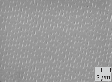
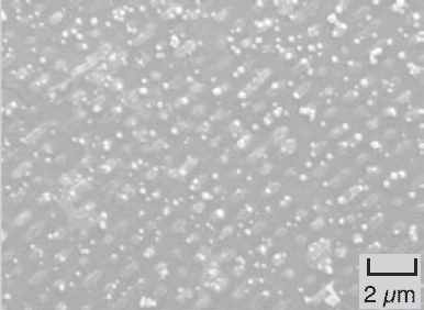
Since electrodeposition occurs at the defect sites, arrays of palladium nanoparticles have been synthesized19 by electrodepositing them on the surface of an aluminum layer obtained from a digital video disc (DVD) that usually has a 50 µm thick aluminum layer between two polycarbonate layers. The aluminum layer with arrays of laser holes was exposed by peeling off one polycarbonate layer, and palladium nanoparticles from a palladium chloride solution were electrodeposited on the holes. Pits in the aluminum layer were created during data recording, and palladium nanoparticles preferentially deposited into the pits, making arrays of metallic nanoparticles. The blank aluminum template and the aluminum template with arrays of electrodeposited palladium nanoparticles are depicted in Figures 2a and 2b, respectively.
|
|
|
|
 |
 |
 |
| a | b | |
|
Figure 2. Scanning-electron micrographs of an aluminum template (a) blank and (b) with electrodeposited arrays of palladium nanoparticles. |
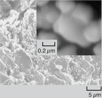
Figure 3. Scanning electron micrographs of palladium particles on a freshly cleaved graphite surface. |
|
|
|
|
|
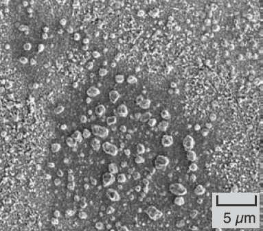
In order to study the role of electrode surface on electrodeposition, palladium nanoparticles were deposited on a freshly cleaved graphite surface.20 A microscopic investigation found that the palladium nanoparticles were faceted and their shape was mostly spherical, as shown in Figure 3. The faceted characteristic of these particles is more clearly observed in the inset of Figure 3. Nuclei formed at almost all parts of the electrode surface; however, the presence of a large number of nanoparticles near the edges and boundaries (Figure 3) indicates a preferential nucleation process.
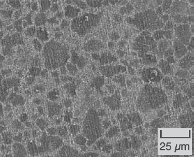
In another study,21 the growth of the palladium nuclei was found to be at the grain interior during electrodeposition on an AISI 316 grade stainless-steel electrode. It is well known that nucleation occurs preferentially at the holes or disorder state of the substrate on which the metal is to be deposited. Scanning electron micrographs of the surface of the stainless steel after electrodeposition of palladium nanoparticles at low and high magnifications are shown in Figures 4a and 4b, respectively. Although nucleation occurred preferentially at the grain boundaries, the extensive growth took place only for nuclei within the grain interior, as shown in Figure 4b. The probable reason for the discrepancy in deposition of palladium particles on the grain rather than on the grain boundary is the presence of oxide ridges at the grain boundaries where the formation of chromium oxide is easy at room temperature. Stainless steel consists of 18 wt.% chromium, which forms thin film oxides at room temperature. The oxidation process is more favorable at the grain boundaries because the formation of oxide nuclei at room temperature is energetically favorable due to the presence of defects. Although the formation of nuclei on such stainless-steel templates during electrodeposition of palladium was easy, subsequent growth of nuclei on top of the oxide ridge at the grain boundaries of the steel substrate was slow compared to that of the nuclei at the grain interior. The slow growth rate was attributed to the difficulty in the charge transfer due to the presence of highly resistive oxide film underneath the nuclei at the grain boundaries of the stainless-steel template.
|
|
|
|
 |
 |
 |
| a | b | |
|
Figure 4. Scanning electron micrographs (a) bare and (b) palladium-deposited stainless-steel surfaces after thermal etching. |
Figure 5. A scanning electron micrograph of palladium particles on carbon tape. |
|
|
|
|
|
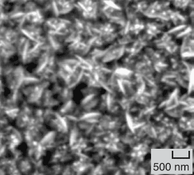
Figure 5 presents the role of amorphous carbon substrate as a template for the electrodeposition of palladium nanoparticles.20 Although the template consists of carbon, the shape of the electrodeposited metallic particle differs from that of the cleaved graphite surface. In the case of the amorphous carbon substrate, the nuclei formed at random locations and fractal growth behavior was observed. In addition, the attachment between the deposits and carbon substrate was weak. All these results strongly indicate that the surface of the active template plays an important role in shape and size distribution of metallic nanoparticles during electrodeposition. Table I presents the various active template substrates used for template-assisted electrodeposition of metallic nanostructures of mostly precious metals such as silver, gold, platinum, and palladium.
|
|
||||
|
Template Substrate
|
Elements Deposited
|
Size and Shape of Nanostructures
|
Ref.
|
|
|
Highly oriented
|
||||
| pyrolytic | ||||
| graphite (HOPG) |
|
|||
|
|
||||
| |
||||
| |
||||
| |
||||
| |
||||
| |
||||
| Graphite surface | |
|||
| |
||||
| Al foil with laser hole | |
|||
| Stainless-steel grain interior | |
|||
| Carbon tape | |
|||
|
|
||||
Restrictive Template-Based Electrodeposition
Another template-assisted synthesis of mostly metal nanowires involves the deposition of metal into the cylindrical pores or channels of an inert, nonconductive nanoporous electrode material. Track-etch membranes,22 porous alumina,23 and other nanoporous structures including conductive polymers, metals, semiconductors, carbons, and other solid materials have been used as templates to prepare nanometer-sized particles, fibrils, rods, and tubules. Various electrode substrates used for restrictive template-assisted electrodeposition of metallic nanostructures are presented in Table II.
|
Table II. Various Restrictive Template Substrates Used for Electrodeposition of
Metallic Nanostructures
|
||||
|
Template Substrate
|
Deposited
|
Size and Shape of Nanostructures
|
Ref.
|
|
| Nanoindented holes | ||||
|
Polyethylene glycol
|
|
|
|
|
| and polyvinyl | |
|
|
|
| pyrrolidone | |
|
|
|
| Semiconductor InAs | |
|
|
|
| quantum well | |
|
|
|
| Mesoporous silica | |
|
|
|
| |
|
|
||
| |
|
|
||
|
|
||||
Palladium deposits with high specific surface areas, up to 50 m2g–1, have been synthesized24 from palladium chloride solutions with additions of polyethylene glycol and polyvinyl pyrrolidone. Details of the globular structure of the deposits depend on the polymer additives. A comparison with electrochemically determined true surface areas demonstrates the rare coalescence of nanoparticles.
|
|
 |
|
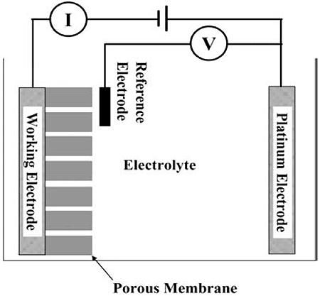
Figure 6. A schematic electrode arrangement for the synthesis of nanowires though restrictive template-assisted electrodeposition. |
|
|
Fasol and Runge25 deposited magnetic permalloy (Ni-Fe) nanowires on the edge of an InAs quantum well. Carrey et al.26 used a nanoindented Al2O3-Al foil to preferentially electrodeposit Ni-Fe nanoparticulate arrays from an electrodeposition bath containing a solution of nickel and iron sulfate. Fabrications of arrays of nickel and cobalt nanowires have been reported through electrodeposition at constant potential by Whitney et al.27 In order to fabricate arrays of nanowires on a polycarbonate porous membrane, a copper film was first sputter-deposited to make the working electrode. The electrodeposition solution was confined to the bare side of the membrane so that deposition was initiated onto the copper film through the pores. It was observed27 that the electrodeposition current was directly proportional to the area of electrodeposits at any given potential under a pseudo-steady-state condition. Thin films composed of ordered arrays of palladium nanowires have been electrochemically synthesized28 using silica mesoporous channels. The experimental set-up showing the electrochemical cell along with a restrictive template for electrodeposition is schematically presented in Figure 6. Mesoporous channels have been deposited on a conductive glass substrate. In this method, nanowires with the face-centered-cubic crystal structure (Fm3m) are continuously deposited from the conductive substrate upward until the mesoporous channels are filled.
The surface morphology of the electrodeposits depends on the structure and chemical composition of the electrode surface as well as other electrochemical parameters. The morphologies of the nanostructures prepared using electrodeposition techniques are usually characterized using transmission electron microscopy and non-contact atomic force microscopy. The electrodeposition of gold12 on HOPG from acidic aqueous solutions was studied by using electrochemical techniques complemented with ex-situ scanning tunneling microscopy. The kinetics of gold electrodeposition are consistent with a nucleation and three-dimensional growth process. A model including a potential-dependent energy barrier at step edges accounts for the morphology transition for gold electrodeposition on HOPG. It was shown12 that dendritic aggregates are produced when the gold surface is negatively charged at potential less than the potential of zero charge. Such growth behavior results from the anisotropic corner surface diffusion caused by the varying energy barriers for the diffusion of surface atoms at step edges, as has been observed for metal deposition from vapor. Rounded kinked gold crystals are formed when the gold surface is positively charged at potential greater than the potential of zero charge. This was attributed to the leveling and lowering of barrier heights at step edges induced by Cl– ion adsorption on gold aggregates. A potentiostatic-pulse method was used11 to electrochemically deposit silver nanocrystallites on the atomically smooth graphite basal-plane surface. The particles were disc-shaped and well separated, with a height of 1.5–5 nm and an apparent diameter of 20–60 nm.
It has been often found that the result of electrodeposition using a carbon substrate is weaker than that with a metallic substrate. The surface morphologies of the nanostructures that are formed on carbon substrates have been found to be faceted.
Template-assisted electrodeposition is a versatile technique to synthesize various kinds of arrays, nanoparticles, and nanowires with a desired structure. Its flexibility gives the opportunity to have nanomaterials of desired surface morphologies.
The synthesis of nanostructures using template-assisted electrodeposition is an emerging area in nanoscience and technology with the possibility of numerous applications in micro and nanodevices. Although a variety of templates and electrodeposition processes are reported in the literature, the universal application of such templates for depositing metallic nanostructures with controlled and well-defined morphologies is missing. The major problem with using electrodeposition to synthesize nanostructure is the preparation of proper templates. Electrodeposition is highly influenced by the surface characteristics of the electrode substrate, and the shape and size of the deposit depend on the substrate. Therefore, further study of electrode surfaces and subsequent surface engineering are essential to develop active templates for the successful synthesis of nanostructures using electrodeposition. In order to understand the preferential deposition on a particular site of the electrode substrate, further studies on the fundamentals of the nucleation and growth of nanoparticles are needed.
The authors acknowledge NASA Glenn, Florida Solar Energy Center— University of Central Florida, Florida Space Grant Consortium for funding the arrayed nanostructure research. S. Seal further acknowledges the Office of Naval Research—Young Investigator Award (ONR YIP-2002), the National Science Foundation, and Department of Defense, Department of Energy, and NASA Small Business Innovation Research Phase I and II through Plasma Process for funding nanotechnology research.
References
1. J. Hu, T.W. Odom, and C.M. Lieber, “Chemistry and
Physics in One Dimension: Synthesis and Properties
of Nanowires and Nanotubes,” Accounts of Chemical
Research, 32 (1999), pp. 435–445.
2. C.M. Lieber, “One Dimensional Nanostructures:
Chemistry, Physics & Application,” Solid State
Communication, 107 (1998), pp. 607–616.
3. C.R. Martin, “Membrane-Based Synthesis of
Nanomaterials,” Chemistry of Materials, 8 (1996),
pp. 1739–1746.
4. A. Huczko, “Template-Based Synthesis of Nanomaterials,” Applied Physics A, 70 (2000), pp. 365–376.
5. C. Suryanarayana, “The Structure and Properties
of Nanocrystalline Materials: Issues and Concerns,” JOM, 54 (9) (2002), pp. 24–27.
6. A. Milchev, S. Stoyanov, and R. Kaischew, “Atomistic
Theory of Electrolytic Nucleation: I,” Thin Solid Films, 22 (1974), pp. 255–265.
7. A. Milchev, Electrocrystallization Fundamentals of
Nucleation and Growth (Boston: Kluwer Academic
Publishers, 2002).
8. B. Scharifker and G. Hills, “Theoretical and Experimental
Studies of Multiple Nucleation,”
Electrochimica
Acta, 28 (1983), pp. 879–889.
9. L. Vázquez et al., “Scanning Tunneling Microscopy
and Scanning Electron Microscopy Observations of
the Early Stage of Silver Deposition on Graphite Single
Crystal Electrodes,” Journal Physical Chemistry, 96
(1992), pp. 10454–10460.
10. R.T. Pötzschke et al., “Nanoscale Studies of
Electrodeposition on HOPG (0001),” Electrochimica
Acta, 40 (1995), pp.1469–1474.
11. J.V. Zoval et al., “Electrochemical Deposition of
Silver Nanocrystallites on the Atomically Smooth
Graphite Basal Plane” Journal of Physical Chemistry,100 (1996), pp. 837–844.
12. H. Martín et al, “Growth Mode Transition Involving
a Potential-Dependent Isotropic to Anisotropic Surface
Atom Diffusion Change. Gold Electrodeposition on
HOPG followed by STM,” Langmuir, 13 (1997), pp.
100–110.
13. M.P. Zach, K.H. Ng, and R.M. Penner, “Molybdenum
Nanowires by Electrodeposition,” Science, 290 (2000),
pp. 2120–2123.
14. Y. Gimeno et al., “Preparation of 100–160-nmsized
Branched Palladium Islands with Enhanced
Electrocatalytic Properties on HOPG,” Chemistry of
Materials, 13 (2001), pp. 1857–1864.
15. Y. Gimeno et al., “Electrochemical Formation of
Palladium Islands on HOPG: Kinetics, Morphology, and
Growth Mechanisms,” Journal of Physical Chemistry
B, 106 (2002), pp. 4232–4244.
16. F. Favier et al., “Hydrogen Sensors and Switches
from Electrodeposited Palladium Mesowire Arrays,”Science, 293 (2001), pp. 2227–2231.
17. J.V. Zoval et al., “Electrochemical Preparation of
Platinum Nanocrystallites with Size Selectivity on Basal
Plane Oriented Graphite Surfaces,” Journal of Physical
Chemistry B, 102 (1998), pp. 1166–1175.
18. M.P. Zach and R.M. Penner, “Nanocrystalline
Nickel Nanoparticles,” Advanced Materials, 12 (2000),
pp. 878–883.
19. D. Bera et al., “Palladium Nanoparticle Arrays Using
Template-Assisted Electrodeposition,” Applied Physics
Letters, 82 (2003), pp. 3089–3091.
20. D. Bera, S.C. Kuiry, and S. Seal, “Dependence
Electrodeposited Nanoparticles on Electrode Surface,”(unpublished).
21. D. Bera, S.C. Kuiry, and S. Seal, “Kinetics and
Growth Mechanism of Electrodeposited Palladium
Nanocrystallites,” Journal of Physical Chemistry B (in press).
22. J.C. Hulteen and C.R. Martin, “A General Template-Based Method for the Preparation of Nanomaterials,”Journal of Materials Chemistry, 7 (1997), pp.
1075–1087.
23. M. Platt, R.A.W. Dryfe, and E.P.L. Roberts,“Electrodeposition of Palladium Nanoparticles at
the Liquid-Liquid Interface Using Porous Alumina
Templates,” Electrochimica Acta, 48 (2003), pp.
3037–3046.
24. G.A. Tsirlina et al., “Quasitemplate Synthesis of
Nanostructured Palladium Electroplates,” Electrochimica
Acta, 47 (2002), pp. 3749–3758.
25. G. Fasol and K. Runge, “Selective Electrodeposition
of Nanometer Scale Magnetic Wires,” Applied Physics
Letters, 70 (1997), pp. 2467–2468.
26. J. Carrey et al., “Electrical Characterization of
Noncontacts Fabricated by Nanoindentation and
Electrodeposition,” Applied Physics Letters, 81 (2002),
pp. 760–762.
27. T.M. Whitney et al., “Fabrication and Magnetic
Properties of Arrays of Metallic Nanowires,” Science, 261 (1993), pp. 1316–1319.
28. D. Wang et al., “Electrodeposition of Metallic Nanowire
Thin Films Using Mesoporous Silica Templates,”Advanced Materials, 15 (2003), pp. 130–133.
29. P. Aranda and J.M. García, “Porous Membranes
for the Preparation of Magnetic Nanostructures,” 249
(2002), pp. 214–219.
For more information, contact S. Seal, University of Central Florida, AMPAC, Eng1, Room 381, Orlando, Florida 32816; (407) 823-5277; fax (407) 882-1462; e-mail sseal@pegasus.cc.ucf.edu and sseal@mail.ucf.edu.
Direct questions about this or any other JOM page to jom@tms.org.
| Search | TMS Document Center | Subscriptions | Other Hypertext Articles | JOM | TMS OnLine |
|---|