An Article from the June 2004 JOM: A Hypertext-Enhanced Article
|
TMS
ONLINE | TMS
PUBLICATIONS | SITE
MAP An Article from the June 2004 JOM: A Hypertext-Enhanced Article |
|
|
|
|
Warren H. Hunt, Jr. is a technical consultant at TMS. |
Exploring traditional, innovative, and revolutionary issues in the minerals,
metals, and materials fields.
|
| OUR LATEST ISSUE |
|
||
Global Perspectives on Electronic Materials: Challenges and Opportunities |
Electronic materials technology has been the engine of the current information technology age, underlying worldwide economic growth and productivity. In 1965, Gordon E. Moore envisioned the role of integrated electronics in enabling home computers, large-scale communications systems, cell phones, and other products that are commonplace today.1 Likewise, substantial manufacturing productivity gains with a smaller workforce have been possible through the integration of information technology broadly through factory systems, automation, and networks as well as via intelligent manufacturing devices such as computer numerical controlled machine tools and robotics. In the United States, the percentage of manufacturing jobs in the total workforce has declined from roughly 30% to just 15% over the past 50 years, while manufacturing productivity has increased and overall manufacturing output remained constant.2 Sustaining this dramatic progress requires relentless pursuit of new generations of electronic products.
|
|
|||||
|
|
|
|
|||
|
DRAM half-pitch (nanometers)
|
|
|
|
|
|
| DRAM memory size (gigabits) |
|
|
|
|
|
| DRAM cost/bit (micro-cents) |
|
|
|
|
|
| Microprocessor physical gate length (nanometers) |
|
|
|
|
|
| Microprocessor speeds (GHz) |
|
|
|
|
|
|
Source: Semiconductor Industry Association |
|||||
The electronic materials industry has a long history of product improvement. The widely quoted relationship for integration level of the number of components per chip doubling every 24 months that is known as Moore’s Law has been realized for many decades. Coupled with decreasing cost per function, remaining on this track through decreasing the minimum feature sizes used in integrated circuits drives ongoing technological improvement. Defining technological targets and identifying potential roadblocks to achieving those targets has been an area of worldwide cooperation. The International Technology Roadmap for Semiconductors (ITRS)3 has developed a consensus set of targets that permeates the R&D efforts to meet both near-term and long-term objectives.
Table I provides a summary of the main targets, called Technology Nodes in the ITRS, through 2018. The table shows that critical dimension sizes in memory and microprocessors will need to decrease dramatically to stay on the current trajectory of performance improvement. The dynamic random-access memory (DRAM) half-pitch correlates to the width and space in between metal lines connecting DRAM bit cells. The smaller this value, the more DRAM bit cells can fit in a given area. This, in turn, relates to the capacity of the DRAM memory, expressed as gigabits in Table I, and DRAM cost/bit. A second key dimension addressed in the ITRS is the microprocessor physical gate length, which refers to the length of the gate that controls the flow of mobile charges in the underlying silicon as a switch. The shorter the gate length, the faster the switch time becomes, with faster microprocessor speeds, as shown in Table I. The Semiconductor Industry Association notes that achieving the technology targets defined by the ITRS would result in microprocessors that are three times faster by the end of the decade and 12 times faster by 2018. Likewise, memory costs would be 1/8th of today’s cost in 2010 and 1/100th only 8 years later.4
THE INTERNATIONAL TECHNOLOGY ROADMAP FOR SEMICONDUCTORS |
|
|
|
The process of technology roadmapping is one that has seen increasing emphasis as a
result of the double demands of speed of innovation and economic streamlining.4 An active
roadmapping effort over 15 years in the semiconductors area demonstrates the evolution
of the process in response to external stimuli. The 2003 edition of the International
Technology Roadmap for Semiconductors builds on a history of roadmaps developed
by the Semiconductor Industry Association in the form of the U.S. National Technology
Roadmap for Semiconductors in 1992, 1994, and 1997. The 1990s saw the semiconductor
industry become increasingly global, and in 1999, through the involvement of international
industry associations from Europe, Korea, Taiwan, and Japan, the first international
edition was published. The roadmap is developed through the efforts of 13 Technology Working Groups covering areas typical of the sub-activities that span the product flow for integrated circuits, termed Focus Groups, and important supporting activities that overlap with the product flow at multiple critical points, termed Crosscut Groups. Nearly 1,000 people participate in the Technology Working Groups and represent a broad cross section of organizations, as noted in Figure Aa, with global representation (Figure Ab). The International Technology Roadmap for Semiconductors (ITRS) presents an industry-wide consensus on the best current estimate of the industry’s R&D needs out to a 15-year time horizon. A basic premise of the roadmap has been that continued scaling of microelectronics would further reduce the cost per function and promote market growth. The roadmap is geared toward identifying the technical challenges that must be overcome to keep pace with Moore’s Law and other trends. Attainment of the targets will push the fundamental limits of materials and require new processes for their manufacture. Advancements necessary are captured in the ITRS in the form of grand challenges. These are divided into two major categories of enhancing performance and cost-effective manufacturing, which are further divided into time frames of near term (up through 2008) and long term (2009–2018). How successful has the ITRS been for the semiconductor industry? Quoting from the executive summary of the 2003 ITRS, “(i)n the last few years, the ITRS documents have become a truly common reference for the entire semiconductor industry. Indeed, the cooperative efforts of the ITRS participants have fostered cooperation among international consortia, universities, and research institutions around the world. It is hoped that the 2003 ITRS will further contribute to stimulate cooperative R&D investments so that the financial burden can be more uniformly shared by the whole industry. It is also hoped that the 2003 ITRS will continue to stimulate the fundamental elements that encourage innovation in individual companies.” Globalization, collaboration, innovation . . . the experience of the International Technology Roadmap for Semiconductors has much to teach in all areas of market-driven materials technology development. 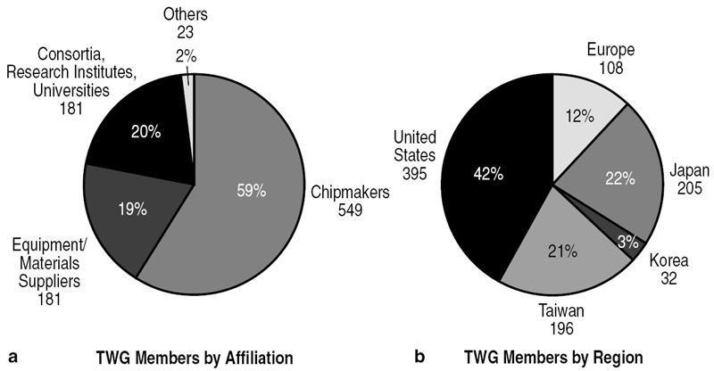 |
|
Figure A. The composition of the technology group—936 global participants.
|
|
INNOVATIVE ECOSYSTEMS |
|
|
|
Clearly there is significant worldwide collaboration in the semiconductor area.
Evidence is the joint activity in the development of the International Technology
Roadmap for Semiconductors as well as the evolution of industrial cooperation through
what is now known as International SEMATECH, the latter having started as a solely
U.S.-government-leveraged activity. Figure B provides a perspective on the global dimension of the electronic materials field. This figure shows the consumption of semiconductors and indicates the dominant role of the Asia Pacific region since 2001. Manufacturing is routinely carried out on a global basis, with labor cost often being the driver. Research and development activities are also beginning to migrate, with increasing emphasis on processing research in Asian countries. While fundamental material R&D is still focused primarily in the United States and Europe, there is growth in this area in Asian countries as well. Looking to the future, continued development of worldwide R&D capabilities coupled with manufacturing in the electronics area may bring about fundamental changes. A recent report2 describes the concept of innovation ecosystems consisting of basic R&D, pre-competitive development, prototyping, product development, and manufacturing in which successful avenues of R&D are assisted by the proximity of the manufacturing processes. The report notes that locations that possess strong R&D facilities as well as manufacturing capabilities are expected to have a competitive edge in innovation. A key component of the ecosystem is the human element as a connection between research and manufacturing. The availability of plentiful educated and skilled workers has been a primary competitive advantage for the United States, but this advantage erodes as the quality of academic and training programs in other countries improves. While this innovation ecosystem model applies to any manufacturing sector, it is considered especially relevant to the information technology area partly because of the short development cycle times and the greater benefit of proximity. Nevertheless, just as the electronics area tends to lead many development trends in the product area, so too does it provide an early view of the changing world order for innovation globally. Nations that are capable of not only manufacturing commodity products with low-cost labor but developing the fundamental capacity for the full spectrum from R&D to manufacturing will compete for technology leadership through innovating new products and new industries. Increasingly we can expect to see multinational companies establish not only their manufacturing plants but also R&D and design centers on an increasingly global basis, changing the industrial ecology as well. 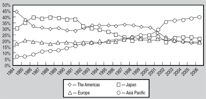 |
Figure B. The percentage share of gobal semiconductor consumption.
|
|
Environment, safety, and health (ESH) issues are becoming an increasing focus in the electronic materials area, and impact both current and future material and process choices and development. With the rapid introduction of new chemicals, materials, and processes, assessment methodologies are needed to ensure that ESH impacts are minimized. While currently the industry is in a reactive stance in this area, more proactive efforts and an ESH-design focus for future materials and processes is envisioned. One specific example of the kind of proactive consideration of these issues needed is the accompanying article by Murr et al. on the evaluation of nanomaterials in the environment and potential health implications.
Environment, safety, and health issues are also important in the packaging area. The Restriction of Hazardous Substances (RoHS), set to go into effect in the European Union in July 2006, is driving the elimination of lead from electronic components. One area that has been the focus of significant R&D has been in the area of lead-free solders. A series of articles in this issue addresses some of the materials and processing issues related to the Sn-Ag-Cu system. Also, the development of halogen-free polymer materials that eliminate brominated flame-retardant substances in sealants and printed wiring boards has been an area of focus and substitutions are expected in Japan and Europe.
The ITRS highlights materials modeling as a grand challenge focusing on the modeling of processing and electrical properties of new materials. It notes that “new materials need to be introduced due to physical limits which otherwise would prevent further scaling. Computational materials science needs to be developed and applied to contribute to the assessment and selection of new materials in order to reduce the experimental effort.”
The modeling challenge is increased by the system complexity at the assembly and packaging level. An example of the complexity of systems involved is the joining of metal, organic, and dielectric materials systems that must adhere during the solder-reflow process. With diverse materials having different coefficients of thermal expansion and solders that are heated to 0.9 Tm or higher during the process, accommodating the resulting thermal stresses becomes a significant challenge. New solder systems that have reflow temperatures roughly 30°C above current systems will add new challenges, especially since current solders are fully liquid at these temperatures. Alternatives such as metal-filled polymers are being considered, but key questions regarding their electrical properties, especially in RF systems, are yet to be answered.
Modeling of the thermal and stress performance of the package is also important. For example, heat transfer between the chip and package is critical to optimize materials and design to keep active areas of the chip cool enough to function properly. Also, it is increasingly important in RF and mixed-signal applications, where the inductance and capacitance of interconnections are important design parameters. While modeling can be a useful guide in these problems, the complexity of the requirements involved still necessitates extensive experimental testing and verification for commercial systems.
The semiconductor industry is a research-intensive one. Traditionally, this industry has invested roughly 15% of sales in R&D, and the recent Battelle R&D forecast5 projects that $15.42 billion will be spent in the United States alone in R&D in 2004. Much of the spending is on the shorter-term development work carried out by industry. One approach to meeting the near-term development needs is industrial consortia such as International SEMATECH, with the goal of ensuring the timely availability of the materials, tools, and technology needed to meet the ITRS objectives. Current International SEMATECH efforts involve six key focus areas of 157 nm lithography, mask cost and availability, next-generation lithography, low κ dielectrics, future gate stack, and manufacturing effectiveness. These pre-competitive programs track with the near-term ITRS objectives.
Longer-term needs of the semiconductor industry have traditionally been addressed through cooperation between industry, the academic community, and government. With the ITRS recognition that current semiconductor device technology will reach its limits in 10–15 years, research in fundamental device physics and properties of new materials have increasing urgency. Universities play an important role in providing fundamental knowledge to address future needs, and nearly half a billion dollars have been spent on university research over the past two decades.6 Research at universities in the United States is coordinated through the Focus Center Research Program. The objective of this program is to concentrate attention and resources on areas of microelectronics research that must be addressed to maintain the historic productivity growth curve of the industry. Currently, 31 U.S. universities are involved in five Focus-Center areas related to the ITRS, specifcally interconnects; design and test; materials, structures, and devices; circuits, systems, and software; and nanomaterials. In addition to generating new research results, the program is intended to strengthen the university research infrastructure and expand its capabilities in silicon-related research.
The materials specialist has an especially challenging assignment in the electronic materials world. While the overarching paradigm that chemistry and processing combine to produce microstructure, which in turn determines properties and performance, certainly holds, electronic materials systems present extreme challenges based on the complexity and small length scales of the system, the diversity of material requirements ranging from mechanical to thermal to electrical, and the dual drivers of a short development time scale and focus on cost. As a result, modeling and simulation generally are an integral part of the design and manufacturing process. Electronic materials specialists, therefore, are involved in a dynamic, entrepreneurial environment. Working within the short development cycle encourages the materials specialist to respond quickly and collaborate to obtain needed information. This model is increasingly relevant in the more traditional materials areas, where product development cycle times are also decreasing.
An initial inspiration for this article was the JOM Roundtable of nine years ago titled “Experts Consider the Future of Electronic Materials” [JOM, 47 (3) (1995), pp. 64–65.] The author appreciates the insights provided by a number of TMS members with expertise in electronic materials, including some who were featured in the 1995 article. Specifically, input was provided by:
- Darrel Frear, Final Manufacturing Technology Center, Freescale Semiconductor (a Motorola subsidiary)
- Martin Weiser, Materials Development manager, Packaging Solutions, Honeywell Electronic Materials
- Sungho Jin, Department of Mechanical and Aerospace Engineering, director, University of California, San Diego Materials Science and Engineering Program
- Jagdish Narayan, Department of Materials Science and Engineering, director, National Science Foundation Center for Advanced Materials and Smart Structures, North Carolina State University
- Bruce Wessels, Department of Materials Science and Engineering, Northwestern University
- Lionel Kimerling, Department of Materials Science and Engineering, director, Materials Processing Center and Microphotonics Center, Massachusetts Institute of Technology
For more information, contact W.H. Hunt, Jr., TMS, 184 Thorn Hill Road, Warrendale, PA 15086; email: whunt@tms.org.
Direct questions about this or any other JOM page to jom@tms.org.
| Search | TMS Document Center | Subscriptions | Other Hypertext Articles | JOM | TMS OnLine |
|---|