 Presenting a Web-Enhanced Presenting a Web-Enhanced Feature Article from JOM |
 LATEST ISSUE |
|||
TMS QUICK LINKS: |
• TECHNICAL QUESTIONS • NEWS ROOM • ABOUT TMS • SITE MAP • CONTACT US |
JOM QUICK LINKS: |
• COVER GALLERY • CLASSIFIED ADS • SUBJECT INDEXES • AUTHORS KIT • ADVERTISE |
|
| Scanning Probe Microscopy for Materials Science | Vol. 59, No.1, pp. 12-16 |
Tip Dilation and AFM Capabilities in the
Characterization of Nanoparticles
Ch. Wong, P.E. West, K.S. Olson, M.L. Mecartney, and N. Starostina
| ||||||||||||||||||||||||||||||||||||
| ||||||||||||||||||||||||||||||||||||
Questions? Contact jom@tms.org. © 2006 The Minerals, Metals & Materials Society |


|
Scanning-probe microscopy has been routinely employed as a surface characterization technique for more than 20 years. Tip deconvolution, the longest-standing problem associated with particle image analysis in atomic force microscopy (AFM), can be solved by scanning a pre-characterized nanosphere prior to imaging unknown particles. INTRODUCTION Knowledge of particle size, size distribution, and other particle morphology parameters on the nanometer scale is becoming more important with accelerating developments in the nanotechnology branches of particle technology, toxicology, pharmaceutical, semiconductor, composite, and coating industries. For example, monitoring the presence of particles, powder size, and distribution data is an important aspect of process control. Changes in these aspects and/or the direction of such changes can be quite indicative of events during the manufacturing process, events which can significantly impact the properties and quality of the final product. Tracking such changes can also indicate the point in the manufacturing process at which there is a problem. Particles and particle-size distribution (PSD) significantly contribute to the mechanical strength as well as thermal and electrical properties of the final material. Smart coatings with a great variety of properties can be developed to meet specific requirements of particular applications. Mechanisms of agglomeration, adhesion, and particle-particle interaction in particulate materials need to be understood to solve current challenges in the pharmaceutical industry.
The most common set of morphology parameters is listed in Table I. Parameters involving measurements of the third dimension such as height, surface roughness, and volume are possible only with atomic-force microscopy (AFM).
The ability to visualize and directly measure dimensions of a few nanometers is a necessity in nanotechnology. There are few particle analysis techniques capable of delivering morphological information below 100 nm. Ensemble methods, such as dynamic light scattering and gravitational sedimentation techniques, are starting to push the limits of resolution at about the 40 nm to the 100 nm range, respectively.1
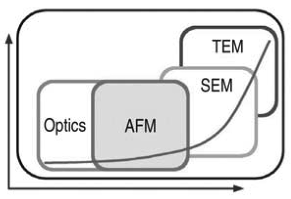
In certain cases, it is important to ensure that PSD lies within certain limits, making the precision of these measurements more important than their accuracy. Microscopy-based techniques, where counted particles can be visually examined, are usually used for absolute measurement applications. Because the resolution of the measuring technique should be greater than the size of the particles under investigationin other words, less than 1100 nmoptical microscopy is excluded (see Table II). However, both AFM and scanning-electron microscopy/transmission-electron microscopy (SEM/TEM) have the required resolution. In fact, AFM is a non-intrusive technique with resolution greater than or comparable to that of an electron microscope. In addition, it is easier to use and involves less sample preparation (see Figure 1). Particles can be measured at ambient condition, while electron microscopy requires vacuum chambers and conductivity of the specimen (see Table II).
Probe artifacts in the case of optical
and electron microscopy, such as aberration,
astigmatism, and distortion, are well
known, studied, and mostly compensated
for in the commercially available microscope.
Note that theoretical resolution
in TEM cannot be obtained, primarily
due to the spherical aberration of the
lens.2 A tip artifact or a tip dilation, the
phenomenon specific to AFM, manifests
itself in a broadening of the lateral
dimensions of the surface topography.
Interestingly, the vertical resolution of
AFM is not affected by the finite size of
the probe. In mathematics, this problem
is known as tip deconvolution. Imaging
very sharp vertical surfaces (those with
high relief) is influenced by the sharpness
of the tip. Only a tip with sufficient
sharpness and aspect ratio can properly
image a given vertical or horizontal
profile. Some profiles can be steeper or
sharper than any tip can be expected to
image without artifact. False images are
generated that reflect the convolution of
the tip geometry and the geometry of
the object being imaged, rather than the
object surface. Mathematical methods
of tip deconvolution can be employed
for image restoration.36 The effectiveness
of these methods depends on the
specific characteristics of the sample and
of the probe tip. A known tip implies a
known sample; if this is the case, then
the morphological subtraction3,4 or
envelope method5 can be used. If the
sample is unknown, then the method of
blind reconstruction can be utilized.3,6
It has been shown that the combination
of erosion with blind reconstruction can
produce the most optimum deconvolution
results on a known sample.4 The
major obstacle in AFM, a tip artifact
associated with the finite size of the
probe, can be compensated for by using
a deconvolution method before performing
analytical measurements. (Note that
all AFM images shown in this paper
are obtained on Nano-Rp: Nanoflat
substrates are used for the sample
preparation; and AFM image analysis
is performed in NanoRule + particle
analysis software.) TIP RECONSTRUCTION ON A PARTICLE SAMPLE It is possible to reconstruct tip geometry on both known and unknown samples. This article will focus on known samples. To refer to a sample as known implies that the size and geometry of particles used as tip characterizers can be independently verified. From a mathematical perspective, it is important to be aware of errors associated with a known sample. Naturally, it is desirable to have a minimum of such errors. The errors in the estimate of characterizer dimensions propagate to comparable errors in the reconstructed tip shape. The characterizer should be stable at the nanoscale with dimensional errors that are small compared to the tip size. Commercially available probes have tip diameters at about 2030 nm. However, there are some special probes with tip diameters as small as 1 nm.
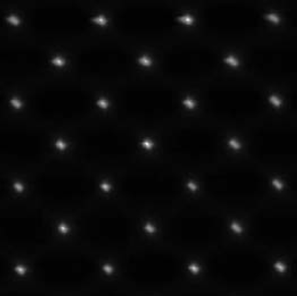
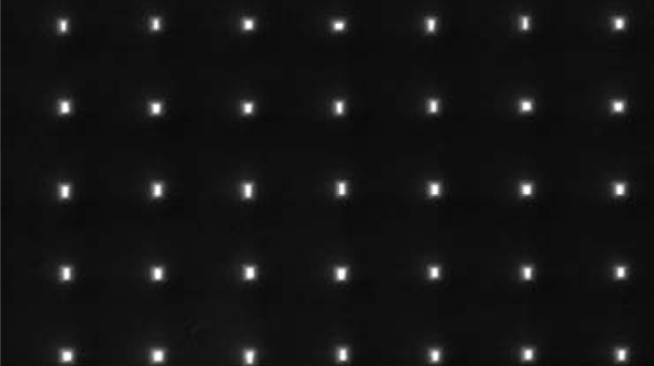
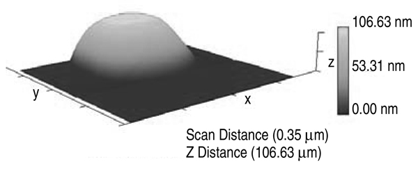
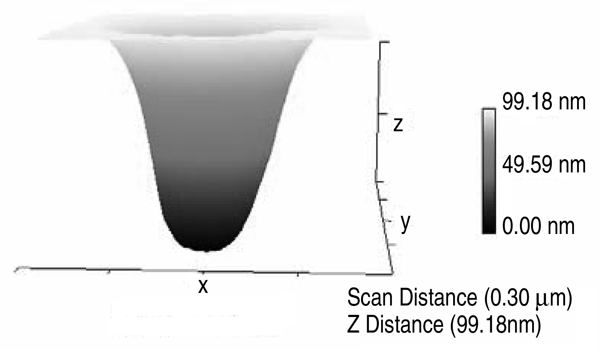
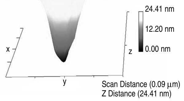
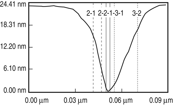
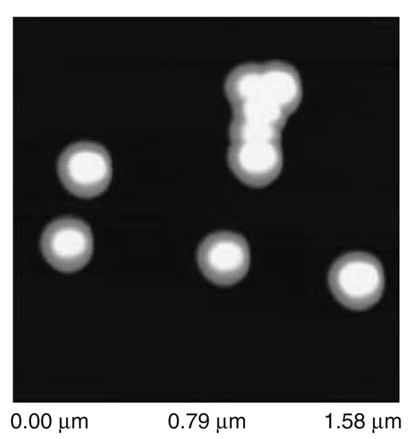
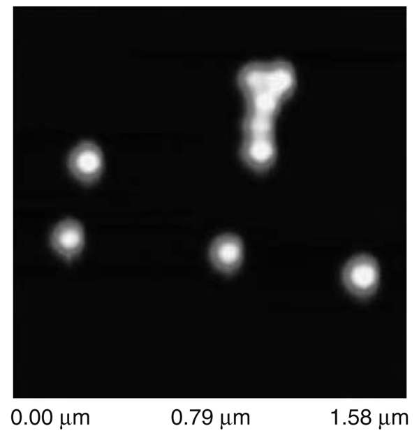
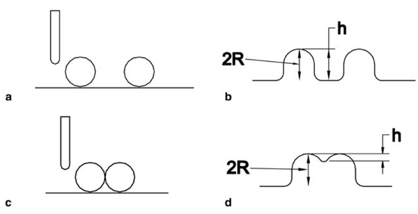
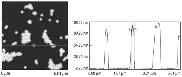
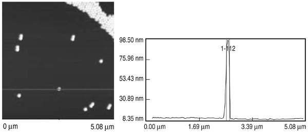
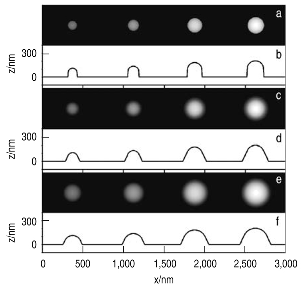
Patterned silicon wafers are routinely used for dimensional calibration of AFM. National Institute of Standards and Technology traceable gratings are available from VLSI Standards, Inc., of San Jose, California. The grid consists of an array of alternating bars and spaces with uniform pitch in both X and Y directions. The uncertainty associated with the pitch size is comparable to the size of the probe. The reported value is on the order of 20 nm for a 2.99 μm pitch. Note that the size of the square impression is about 1.5 µm × 1.5 μm. The calibration grating consisting of an array of sharp tips, with strict symmetry on tip sides, small cone angle (less than 20°), and small curvature radius of the tips (less than 10 nm) is a very good candidate for determination of styli shape parameters11 (NT-MDT, Moscow). However, the lack of specifications for the parameters mentioned and the complicated shape of the spikes makes the problem more complicated. Figure 2 shows an AFM image of the pillars in comparison to the SEM image. Both AFM and SEM data agree that the spikes appear to have variations in shape and size. The use of single spherical particles has been proposed for tip characterization for several reasons. The high degree of symmetry, manufacturability, consistent uncertanties on the scale of 13 nm, noncompressibility, negligible elastic deformation, and conformation on the substrate make colloidal gold and polystyrene particles favorable candidates for tip geometry checkers.3,4,9,12 Figure 3 shows one example of a three-dimensional view of a tip reconstructed from an AFM image of a 102 ± 3 nm polystyrene sphere. The reconstructed tip appears to be asymmetrical in shape with a tip radius of ~38 nm, a left angle of 65°, and a right angle of 50° (Figure 4). The reconstructed tip obtained on scanning 28 nm colloidal gold spheres (Ted Pella, Inc., Redding, California) is shown on Figure 5. The tip has a radius of ~2 nm, a left angle of 58°, and a right angle of 46°. The reconstructed tip is outer bound on the part of the tip which contacts the particle during the scan. This happens due to the fact that dilation and erosion operators are not strict inverses of one another for an arbitrary tip.4 The closing operation tends to smooth the edge from the outside. The tips outer bound estimate is the more important one because it leads to a lower bound estimate of the sample surface.3 SURFACE RECONSTRUCTION Once the geometry of the tip is estimated, it is possible to reconstruct the surface topography. Figure 6 shows AFM images of the particles before and after reconstruction. Ideally, if a tip is perfectly reconstructed, the reconstructed sample surface will be an outer bound that contains an actual sample. This outer bound will be equal to the true sample surface at those points where the tip actually touched, and it will be larger at points where the tip was unable to touch. Notice that the true particle surface is a cylinder with a hemisphere cap. That is, it contains vertical sidewalls where the tip was not able to touch. This is one of the reasons that these reconstructed samples seem dilated (compare Figures Be, computer-simulated tip dilation, and Figure 6, tip dilation on measured and reconstructed surfaces). AFM RESOLUTION ON PARTICLES The conventional definition of resolution
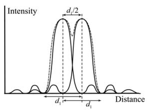
in the field of light and electron
microscopy is based on the Lord Rayleigh
criterion: when the maximum
intensity of an Airy disc coincides with
the first minimum of the second, then
two points can be distinguished.2 This sets the resolution limit as d/2, as shown
in Figure 7. The Rayleigh criterion can
be applied to three-dimentional images
of AFM. Here, the intensity peaks are
analogous to height line profiles. Let us
assume r is tip radii, R is sphere radii,
and h is the height difference between
the top of the sphere and the lowest
point in a line profile drawn through two
spheres. H is the distance that actually
can be measured on the height profile.
These line profile measurements should
be performed on deconvoluted surfaces
to compensate for tip artifact. CONCLUSION In this work, tip deconvolution and image restoration are done on known, pre-characterized manufacturable spheres from a commercial vendor, rather than an arbitrary unknown surface or mathematically modeled structure. This is a practical, innovative solution to the long-standing problem of tip deconvolution. REFERENCES
1. A. Jillavenkatesa, S. Dapkunas, and L. Lum, Particle
Size Characterization (Gaithersburg, MD: NIST, 2001). P.E. West and N.V. Starostina are with Pacific Nanotechnology Inc., 17984 Sky Park Circle, Suite J, Irvine, California 92614. K.S. Olson and M.L. Mecartney are with the Department of Chemical Engineering and Material Science at the University of CaliforniaIrvine. Ch. Wong is with the Claremont Graduate University School of Mathematical Sciences, Claremont, California. N. Starostina can be reached at (949) 253-8813; fax (949) 253-8816; e-mail nstarostina@pacificnanotech.com
|
||||||||||||||||||||||||||||||||||||||||||||||||||||||||||||||||||||||||||||||||||||||||