 Presenting a Web-Enhanced Presenting a Web-Enhanced Article from JOM |
 LATEST ISSUE |
|||
TMS QUICK LINKS: |
• TECHNICAL QUESTIONS • NEWS ROOM • ABOUT TMS • SITE MAP • CONTACT US |
JOM QUICK LINKS: |
• COVER GALLERY • CLASSIFIED ADS • SUBJECT INDEXES • AUTHORS KIT • ADVERTISE |
|
| Low-Dimensional Nanomaterials: Overview | Vol. 62, No.4 pp. 35-43 |
Growth, Properties, and Integration
S.T. Picraux, S.A. Dayeh, P. Manandhar, D.E. Perea, and S.G. Choi
Questions? Contact jom@tms.org. |
|
Semiconducting nanowires are an area of widespread interest in nanomaterials research because of the ability to fabricate one-dimensional structures with tailored functionalities not available in bulk materials. Silicon and germanium nanowires have received particular attention because of the important role played by these materials systems in contemporary microelectronics and their potential for applications ranging from novel electronic devices to molecular level sensing and to solar energy harvesting. This paper provides an overview of the widely used vapor-liquid-solid technique for nanowire growth and its application to our recent silicon and germanium nanowire studies. Nanoscale materials are of great interest because of the possibilities they offer for obtaining new properties at small size. Basically, when structures approach the ~100 nm size regime their properties may change with decreasing size for the same atomic composition. This size dependence derives from three basic effects: surfaces become a large volume fraction of the structure, with those surface atoms having greater energy and different coordination; interfaces between nanostructures become a major component of the structures, with their modified electronic properties, strain gradients, and influence on the flow of defects, charge carriers, phonons, etc.; and sufficiently reduced dimensions lead to quantum size effects and coherent interactions between structures. These size-dependent effects result in changes in the physical properties of nanomaterials as well as changes in the interaction of electromagnetic energy with and transport of energy through nanomaterials. For example, electronic, optical, magnetic, and mechanical properties are altered, chemical reactivities change, new collective properties may emerge for arrays of nanostructures, and electromagnetic fields may be locally enhanced, for example in plasmonic effects. One-dimensional (1-D) structures such as nanowires provide a particularly attractive class of nanomaterials. One can tailor the functionality of nanowires in a variety of ways and their geometry is optimal for achieving new regimes of 1-D transport of charge carriers and heat to realize new devices. Semiconducting nanowires are particularly versatile because of the wide range of properties that can be achieved. Thus much attention has been focused on these structures and their potential applications in such areas as electronic1,2 and photonic devices,3,4 chemical and biomolecular sensing,5,6 and energy harvesting710 and storage.11 Silicon nanowires have especially seen an enormous number of studies over the last decade.12 This attention derives in part because of the simplicity of the growth of these and other nanowires by metal catalyzed chemical vapor deposition techniques and in part due to the importance of Si as an electronic device material. Compound semiconductor nanowires, especially GaAs, InGaAs, InAs, and ZnO, have also been widely studied,4,1214 particularly for their optoelectronic properties such as for light emitting diodes, nanoscale lasing, and photodetector structures, and for their piezoelectric properties. Another class of widely investigated 1-D structures is carbon nanotubes.15 These nanostructures can be either semiconducting or metallic in nature, depending on the orientation at which their graphene sheets are wrapped into a tube. Carbon nanotubes have extremely high electrical conductivity, thermal transport, and strength, and have been considered for applications ranging from arrays for effi cient field emitters to thermal materials, to fillers for structural composites, conductive plastics and adhesives, and electrodes for batteries and capacitors.16 Semiconducting carbon nanotubes are interesting as electronic devices due to their unusually efficient transport characteristics and quantum effects.
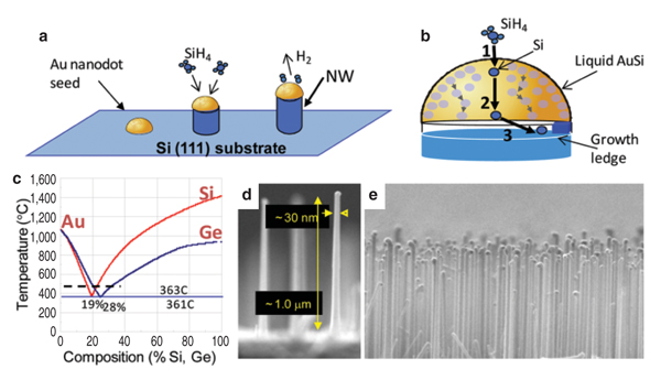
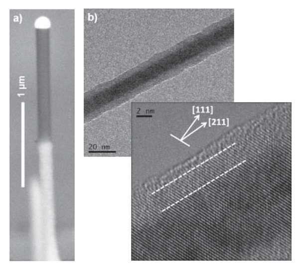
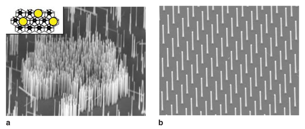
For all these 1-D semiconducting nanomaterials the ability to integrate the structures into larger systems with the necessary manufacturing control and reproducibly, as well as an understanding of the new properties resulting from their surfaces and interfaces, will be critical to their eventual application. Due to the large breadth of the fascinating field of semiconducting nanowires we will restrict our focus here to Si and Ge nanowires. We give an overview of the growth and properties of these materials based on our recent studies and discuss some of the critical issues which must be controlled for their integration into larger scale structures and eventual applications. VLS Growth Technique Figure 1 illustrates the VLS method for Si and Ge nanowire growth. The schematic in Figure 1a shows silane molecules reacting at the Au surface through a hydrogen decomposition reaction sequence that introduces atomic Si into the Au nanodot (Figure 1b). The temperature is held near the eutectic temperature of 363°C and as the composition approaches the eutectic composition of 19 at.% Si (Figure 1c) melting occurs. Upon further addition of Si, the Si concentration in the liquid Au moves to the right of the liquidus line and the supersaturation becomes sufficient for crystallization of Si at the liquid-solid interface. The liquid drop size defines the liquid-solid interface and thus the area available for Si crystal growth. This maintains the nanowire growth at a fixed diameter as long as Au is not lost from the nanodrop. Since Si and Ge exhibit similar eutectic behavior with Au (see Figure 1c), Si, Ge, and SiGe alloy nanowires can all be readily grown by this same approach. Figure 1d illustrates a Si0.1Ge0.9 alloy nanowire. In general, Ge nanowire growth is carried out at ~275 to 375°C18 and Si at 450 to 550°C,19 since Ge precursors are more easily decomposed than Si precursors in the VLS process due to the greater reactivity of germane compared to silane. An important advantage of low growth temperatures is that conventional vapor-solid (VS) CVD growth on the nanowire sidewalls and Si substrate is minimized during nanowire VLS growth. Simultaneous sidewall growth reduces the maximum aspect ratios that can be achieved and results in a linear tapering of the nanowires. Tapering can also occur as a result of the loss of Au atoms from the nanowire tip if there is significant Au surface diffusion along the Si sidewall during growth, however this usually occurs only at ultra-high vacuums and low pressures and is not a consideration for usual CVD reactor growth conditions.20 There are three steps involved in the growth kinetics which combine to establish the nanowire growth rate (see Figure 1b). Step 1 is the decomposition reaction at the vapor-liquid interface which introduces Si into the liquid metal, step 2 corresponds to Si diffusion through the liquid to the solid-liquid interface, and step 3 is the Si crystallization at the liquid-solid interface which adds atoms to the nanowire surface. Typically the growth rates range from below 1 to 10s of nm/s so that the nanowire growth process is rapid. Since diffusion in liquids is fast for the few nanometer distances involved here, the transport in step 2 is rapid and not a limiting factor in the kinetics. The growth rate is then determined in steady state when the rates for step 1 and step 3 are equal and thus in equilibrium, both of which scale with surface area. Since the flux of the gas precursor molecules to the liquid Au surface is directly proportional to pressure, increasing the precursor partial pressure increases the available Si in step 1 and the resulting growth rate increases.21 An increased pressure is equivalent to increasing the chemical potential difference between Si in the vapor and solid phases, which increases the Si concentration in the liquid Au and in turn the Si supersaturation which leads to an increase in the crystallization rate (step 3) at the liquid-solid interface. At larger Au seed sizes (~50 nm and larger) the growth rate is typically constant with nanowire diameter. However, decreasing the Au seed size at sufficiently small diameters increases the chemical potential in the liquid nanodot according to the Gibbs- Thomson effect, reducing both the forward chemical reaction rate introducing Si in step 1 and the crystallization rate in step 3, and thus decreases the growth rate. At sufficiently small Au nanodot diameters the chemical potential rises sufficiently to drop the supersaturation to zero and growth ceases.22 This leads to a minimum diameter for which nanowires can be grown, which for typical growth conditions is ~5 nm. Scanning electron microscopy (SEMs) images in Figure 1d and e shows Si0.1Ge0.9 alloy nanowires ~30 nm in diameter by 1 µm long for individual and dense arrays of nanowires, respectively, grown in a 50% silane and 30% germane in hydrogen gas mixture at a total gas pressure of 3 Torr.23 An important feature of the VLS growth process is that it results in epitaxial growth of single crystal nanowires of high perfection oriented primarily along in the <111> crystal direction for Si and Ge with diameters greater than ~25 nm and along <211> and <110> directions at smaller diameters. The change in growth direction at small diameters is the result of overall energy minimization between the liquid-solid interface energy and the nanowire sidewall energy. The 30 nm diameter <111> oriented wires in Figure 1d and e are vertical because they grew epitaxially from a Si (111) oriented substrate. The VLS growth process does not always lead to straight nanowires. For example, instabilities due to changes in temperature, pressure, or gases present during growth can lead to instabilities in the liquid growth seed on top of the growing nanowire and result in kinking or twining along the growth direction.24 For kinked Si and Ge, the growth often switches between the four available <111> directions which corresponds to a 55° tilt in the wire direction, or to another of the favored growth directions such as the <211> direction at a 19° tilt. In addition to bottom-up VLS growth, top-down methods have also been used to form Si nanowires. They are often based on planar lithography definition of the wire width and length from Si-on-insulator structures.25 Another approach is to lithographically or chemically induced patterning accompanied by preferential etching into an Si substrate to form arrays of vertical structures.9 These top-down methods tend to be more challenging, either in control of the dimensions or due to rough nanowire sidewalls. In contrast, the VLS method has been much more widely used because it provides an easy route for synthesis and allows the growth of a wide variety of semiconducting materials, including Si, Ge, SiC, B, GaAs, GaP, InP, InAs, and ZnO, among others.12
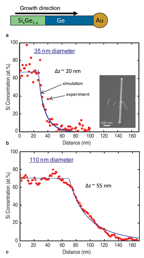
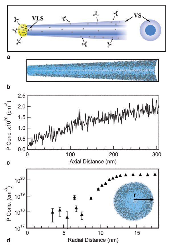
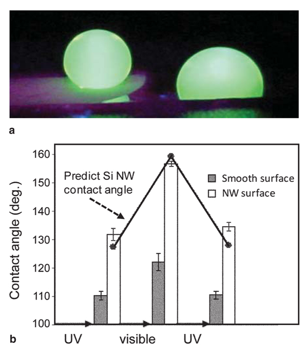
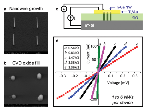
Heterostructure Synthesis Compositional heterostructure growth in the Si/Ge axial nanowire system has been challenging in the VLS growth method due to the instabilities created at the growing liquid-solid interface during switching of the growth precursor gases. This instability can lead to severe kinking of the nanowires and even loss of the liquid Au seed from the nanowire tip upon gas switching. As a result, previous axial Si/Ge heterostructures were typically limited to compositional changes of ~20% or less.29,30 Recently, we have demonstrated Si/Ge nanowire growth with changes extending over the entire SiGe compositional range.31 In Figure 2 compositional profi les for Si at the Si0.3Ge0.7/Si interface are shown for two different nanowire diameters. The abruptness of the interface transition region depends on the diameter, with the smaller diameter having a sharper transition. This chemical transition region for VLS synthesis arises from the liquid Au alloy composition during growth. Upon switching from growth species A to B, the liquid acts as a reservoir for the growth species A which must be depleted from the liquid by subsequent crystallization at the liquid-solid interface while B is added to the liquid for the transition to pure B growth to occur. The solid curve in Figure 2 is calculated based on our simulations, which only assume that the incorporation probabilities for Si and Ge are proportional to their concentrations in the liquid at the nanowire crystallization front (step 3 in Figure 1b). Other studies have shown similar behavior at smaller compositional changes with the width of the transition region proportional to the nanowire diameter.30 In Figure 3 both axial and radial 100% compositional heterostructures are shown for the Si/Ge system.31 We have achieved these dislocation-free structures in both cases by in situ growth in our CVD system, using VLS growth for the axial case and subsequent VS growth for the radial case. For the case of radial VS growth, which will be discussed in more detail in the following section, the composition transition regions can be atomically sharp, provided high growth temperatures which can induce solid phase diffusion across the interface are not used. Electrical Dopant Incorporation A primary consideration in dopant atom incorporation during VLS growth is the control of the dopant spatial distribution, both radially and axially. An important recent advance in this area has been the application of atom probe tomography to obtain 3-D composition profiles of nanowires with the sensitivity needed to measure dopant atom distributions within nanowires at concentrations ~5×10¹⁷/cm3 and higher.32 Figure 4 illustrates this technique for P distributions both along the length of a Ge nanowire and radially from the nanowire center to the outer perimeter. From Figure 4 the issue of simultaneous dopant incorporation by VLS growth in the central region of the nanowire and by VS growth of a heavily doped shell region is clearly illustrated. Differences in dopant precursor decomposition and incorporation rates between the liquid catalyst for VLS growth and the solid nanowire surface for VS growth give rise to a heavily doped shell surrounding an under-doped core. These effects are significant for conventional dopants such as diborane and phosphine in Si and Ge nanowire growth. For example, under some CVD growth conditions VLS growth incorporates Ge into the growing nanowire 20 times more efficiently than VS growth incorporates Ge on the sidewall; in contrast, P is incorporated in the sidewall during VS growth seven times more efficiently than into the nanowire core by VLS growth. This VS sidewall doping effect complicates control of doping along the length of the nanowire, since the doping concentration will depend on the length of time of sidewall exposure to VS growth, and hence the distance from the nanowire tip. Vapor-solid dopant incorporation further complicates the growth of nanowire heterostructures such as an axial p-n junction. For example, during growth of the n-doped segment, the previous p-doped region will have a surrounding n-doped compensating shell via unwanted VS shell growth.33 While lower growth temperatures or post-growth etching can reduce the extent of unwanted VS shell doping, further developments in VLS growth techniques are needed to eliminate this effect if full control over axial nanowire doping is to be achieved. However, one advantage of the incorporation of dopants by VS sidewall growth on nanowires is that radial doping of nanowires is possible. Thus radial p-n junctions can be obtained by emphasizing the VS sidewall growth process (for example, by higher temperatures and lower pressures). Relatively few studies of radial devices, such as for p-i-n solar cells,34 have been demonstrated at this time. Electrical, optical, thermal, and chemical properties are among those of greatest interest for semiconducting nanowires. Electrical transport is modified by the close proximity of the nanowire surface due to charge trapping and scattering with relevance to both minority and majority carrier devices. Diffuse optical scattering of incident light by Si nanowires due to the dielectric constant difference from air gives rise to the dark appearance of a dense nanowire surface. This shortens the distance for light absorption by about an order of magnitude from ~250 μm crystalline Si solar cells to ~10 µm for an array of Si nanowires and is one of the factors which make them of potential interest for photovoltaic applications.35 Thermal transport occurs mainly by phonons in nanowires and the strong phonon scattering at small diameters greatly reduces heat transport through nanowires. This reduction is expected to significantly enhance thermoelectric efficiencies and has sparked interest in nanowires for thermoelectric cooling and electrical current generation applications.9,10 Chemical properties of nanowires are changed in a number of ways due to the large effective surface area for a nanowire-covered surface. For example, Si nanowires can much more readily accommodate the several 100% volume change by radial expansion upon cycling of Li in and out of Si and have the potential to increase the charge storage capacity of Li battery anodes by a factor of 10 if they can be shown to have suffi cient lifetimes.11 Here we briefly discuss two examples for Si nanowires to illustrate their altered electrical and chemical properties from bulk materials. Electrical At higher carrier concentrations surface state effects do not directly give rise to significant depletion into the nanowire, but still have an important influence on electrical transport due to surface scattering and recombination. For example, nanoprobe electrical transport studies across the Au-catalyst/ Ge-nanowire Schottky diode interfaces for n-type electrical carrier doping in the 1018 to 1019/cm3 range have shown electron-hole recombination at the nanowire surface to be the dominant charge transport mechanism.39 The resulting nanowire conductance behavior is strongly influenced and diameter dependent. The extent to which these diameter-dependent changes in electrical transport behavior will be important or be exploited in nanowire electronic applications is not yet known. Chemical The hydrophobicity of surfaces illustrates an area where such surface chemical effects are pronounced. Surface wetting properties of a hydrophobic or hydrophilic surface are well known to be amplifi ed by rough surfaces with their increased surface areas. Since silicon dioxide surfaces are easily modified chemically by functionalizing with a wide variety of molecular species, Si nanowires on a Si substrate with their air oxidized surfaces provide a natural platform to examine such surface chemical effects. Figure 6a contrasts the wetting of a droplet of water on Si nanowire (left side) and smooth Si (right side) surfaces after functionalization with perfluorooctyl-trichlorosilane (PFOS). The wetting angle which is only slightly greater than 90° on the smooth hydrophobic surface greatly increases on the superhydrophobic nanowire surface. Further, if the surfaces are functionalized with a monolayer of photochromic-containing molecules such as spiropyran, the surface bound molecules can be switched between nonpolar and polar forms under visible and ultraviolet (UV) irradiation.40 Thus, light can be used to switch the hydrophobicity of the surface. In this way a nanowire surface morphology has been shown to significantly amplify the light-induced change in water contact angle.40 As illustrated in Figure 6b the change in contact angle between visible and UV irradiation increased from 12° on a smooth Si surface to 23° on the spiropyran-coated nanowire surface, whereas the contact angle hysteresis for water droplet motion on the surfaces decreased from 37 to 17°. As a result, the advancing water contact angle under UV irradiation is lower than the receding water contact angle under visible irradiation, which allowed water droplets to be moved on the roughness-magnified photoresponsive nanowire surface solely by the light-induced lowering of the surface energy. While many types of nano- and microscale surface chemical modifications are used to alter surface energies for applications ranging from petroleum extraction to soil-resistant cloth, this example illustrates the significant effect of the greatly increased surface area for nanowires. Integration has played a pivotal and revolutionary role in the development of nearly all science and technology, with very large scale integrated circuits being one of the most striking examples. Even greater challenges exist as nanomaterials are integrated into new architectures to form functional systems. Nanowire integration leads to the formation of interfaces and surfaces whose structure and properties can dominate the electronic, optical, chemical, and mechanical properties of the system. New directed- and self-assembly approaches must be developed for facile assembly and greater functional control. Combined bottom-up and topdown synthesis and assembly techniques are needed to allow controlled, large-scale formation of micro-scale systems. Establishing these processes for integration of nanowires will be of paramount importance for their application in nanotechnology.
Directed Assembly and Contacting
of Nanowire Arrays
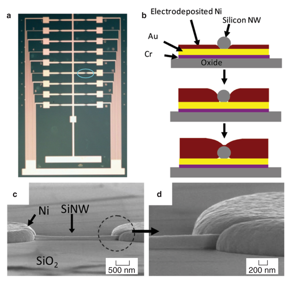
We have explored Si nanowire dielectrophoretic assembly combined with electrodeposition for electrically contacting the nanowires for electrical transport sensor arrays. The focus of these earlier studies was on the contact directed assembly process.43 Figure 7 illustrates this approach for the assembly of the electrical contacts to Si nanowires after dielectrophoretic alignment onto the pre-patterned Au leads. The Si nanowires are, in essence, buried by the electrodeposited Ni. Brief thermal anneals are then required to form good electrical contact to the nanowires. As for the cantilever arrays these methods, which mimic the biological solution-based approach to self assembly, offer the advantage of nanowire manipulation and assembly without further lithography. Further advances in combined bottom-up assembly with top-down patterning are needed, however, if efficient and reproducible manufacturing methods are to be obtained by this approach. Vertical Arrays and Devices
While the vapor-liquid-solid method, commonly used for the growth of semiconductor nanowires, was discovered over 50 years ago, it is only in the last 10 years that a wide range of nano-wire materials, properties, devices, and potential applications have been investigated. Silicon and germanium are among the most widely studied of these materials. For future applications increased control of the synthesis of nanowires, including their nucleation, heterostructure formation, and electrical doping is required. Equally important will be a more indepth understanding of their properties together with the development of architectures and integration approaches to fully exploit their unique properties. Energy applications are one of the recent areas for semiconducting nanowires receiving much attention, due to their potential for new approaches to energy storage in batteries and energy harvesting in solar cells and thermoelectric devices. Progress in these and other application areas will benefit by significant advances in the integration of 3-dimensional arrays of nanowires into micro- and macroscale systems. ACKNOWLEDGEMENTS This work was performed at the Center for Integrated Nanotechnologies, a U.S. Department of Energy, Offi ce of Basic Energy Sciences, user facility. Los Alamos National Laboratory is operated by Los Alamos National Security, LLC, for the National Nuclear Security Administration of the U.S. Department of Energy under Contract No. DE-AC52-06NA25396. REFERENCES 1. C. Thelander et al., Materials Today, 9 (2006), p. 28.2. S.A. Dayeh, Semiconductor Science and Technology, 25 (2010), p. 024004. 3. D.J. Sirbuly et al., Proc. Natl. Acad. Sci., 102 (2005), p. 7800. 4. Y. Li et al., Materials Today, 9 (10) (2006), p. 18. 5. Z. Li et al., Nano Lett., 4 (2004), p. 245. 6. G. Zheng et al., Nature Biotech., 23 (2005), p. 1294. 7. L. Tsakalakos et al., Appl. Phys. Lett., 91 (2007), p. 33117. 8. B.M. Kayes, H.A. Atwater, and N.S. Lewis, J. Appl. Phys., 97 (2005), p. 114302. 9. A.I. Hochbaum et al., Nature, 451 (2008), p. 163. 10. A.I. Boukai et al., Nature, 451 (2008), p. 168. 11. C.K. Chan et al., Nature Nanotech., 3 (2008), p. 31. 12. N. Wang, Y. Cai, and R.Q. Zhang, Mater. Sci. and Eng., R60 (2008), p. 1. 13. N. Skold et al., Nano Lett., 5 (2005), p. 1943. 14. Z.L. Wang, Adv. Mater., 19 (2007), p. 889. 15. M.P. Anantram and F. Leonard, Reports on Progress in Phys., 69 (2006), p. 507. 16. S.B. Sinnott and R. Andrews, Critical Reviews in Solid State and Materials Sciences, 26 (3) (2001), pp. 45 249. 17. R.S. Wagner and W.C. Ellis, Appl. Phys. Lett., 4 (1964), p. 89. 18. H. Adhikari et al., ACS Nano, 1 (2007), p. 415. 19. V. Schmidt et al., Adv. Mater., 21 (2009), pp. 26812702. 20. J.B. Hannon et al., Nature, 440 (2006), p. 69. 21. J. Dailey et al., J. Appl. Phys., 96 (2004), p. 7556. 22. E.I. Givargizov, J. Crys. Growth, 31 (1975), p. 20. 23. S.G. Choi et al., unpublished work (2010). 24. P. Madras, E. Dailey, and J. Drucker, Nano Lett., 9 (2009), p. 3826. 25. D. Wang, B.A. Sheriff, and J.R. Heath, Small, 2 (2006), p. 1153. 26. W. Lu et al., Proc. Natl. Acad. Sci., 102 (2005), p. 10046. 27. J.G. Swadener and S.T. Picraux, J. Appl. Phys., 105 (2009), p. 044310. 28. W.D. Nix, MRS Bulletin, 34 (2009), p. 82. 29. Y.Y. Wu, R. Fan, and P. Yang, Nano Lett., 2 (2002), p. 83. 30. T.E. Clark et al., Nano Lett., 8 (2008), p. 1246. 31. S.A. Dayeh, P. Manandhar, and S.T. Picraux, unpublished work (2010). 32. D.E. Perea et al., Nature Nanotech, 4 (2009), p. 315. 33. E. Tutuc, et al., Nano Lett., 6 (2006), p. 2070. 34. B. Tian et al., Nature, 449 (2007), p. 885. 35. O.L. Muskins et al., Nano Lett., 8 (2008), p. 2638. 36. J. Appenzeller et al., IEEE Trans. Elect. Devices, 55 (2008), p. 2827. 37. S. Ingole et al., J. Appl. Phys., 103 (2008), p. 104302. 38. S. Ingole et al., IEEE Trans. Elect. Devices, 55 (2008), p. 2931. 39. F. Leonard et al., Phys. Rev. Lett., 102, (2009) p. 106805. 40. R. Rosario et al., J. Phys. Chem. B Letters, 108 (2004), p. 12640. 41. N.A. Melosh et al., Science, 300 (2003), p. 112. 42. M. Li et al., Nature Nanotech., 3 (2008), p. 88. 43. S. Ingole et al., Appl. Phys. Lett., 91 (2007), p. 033106. 44. See, for example, P. Nguyen et al., Nano Lett., 4 (2004), p. 651. 45. M.T. Bjork et al., Appl. Phys. Lett., 90 (2007), p. 142110. 46. Y. Sierra-Sastre et al., J. Amer. Chem. Soc., 130 (2008), p. 10488. 47. S.A. Dayeh et al., submitted to Nature (2010). 48. P. Manandhar and S.T. Picraux, submitted to Nano Letters (2010). S. Tom Picraux is chief scientist at the Center for Integrated Nanotechnologies (CINT), Los Alamos National Laboratory, Los Alamos, NM; Shadi Dayeh, Pradeep Manandhar, and Daniel Perea are postdoctoral associates, also at the CINT. Sukgeun Choi is a former postdoctoral associate at CINT and is now a staff member at the National Renewable Energy Laboratory, Golden, CO. Dr. Picraux is also an adjunct professor at Arizona State University. He can be reached at (505) 665- 8554; e-mail picraux@lanl.gov. |