 Presenting a Web-Enhanced Presenting a Web-Enhanced Feature Article from JOM |
 LATEST ISSUE |
|||
TMS QUICK LINKS: |
• TECHNICAL QUESTIONS • NEWS ROOM • ABOUT TMS • SITE MAP • CONTACT US |
JOM QUICK LINKS: |
• COVER GALLERY • CLASSIFIED ADS • SUBJECT INDEXES • AUTHORS KIT • ADVERTISE |
|
| Research Summary: Surface Engineering | Vol. 57, No.12, pp. 60-64 |
The Bonding of Nanowire
Assemblies
Using Adhesive and Solder
ZHIYONG GU, HONGKE YE, and DAVID H. GRACIAS
| ||||||||||||||||||||||||||||||||||||||||
| ||||||||||||||||||||||||||||||||||||||||
| ||||||||||||||||||||||||||||||||||||||||
| ||||||||||||||||||||||||||||||||||||||||
|
Questions? Contact jom@tms.org. © 2005 The Minerals, Metals & Materials Society |


|
However, in many cases, the assembled structures are not well bonded. This paper summarizes results on directing the assembly of metallic rod-shaped (30200 nm diameter) components with one another and with substrates to form structures that can be bonded by adhesive or solder. The methodology can be adapted with other self-assembling strategies to form mechanically stable, and in certain instances electrically conductive, assemblies composed of nanoscale componenents. INTRODUCTION In recent years, the extreme miniaturization of microelectronic, photonic, and micro-electromechanical systems has pushed the capabilities of conventional top-down microfabrication to its limits in terms of cost-effective mass production of devices and integrated systems. New nanofabrication techniques are needed to address the challenges of decreasing dimensions in order to enable the era of nanotechnology. One promising strategy is to direct the assembly of nanoscale components to form two-dimensional (2-D) or three-dimensional (3-D) structures from the bottom up.110 The directed assembly of engineered structures is inspired by biological self-assembly; nature can mass produce complex 2-D and 3-D structures with sizes ranging from the sub-nanometer to the millimeter and beyond. The nanocomponents used in directed assembly are fabricated using either conventional nanolithography11,12 or non-lithographic methods including chemical vapor deposition,13,14 electrodeposition in templates,1517 and molecule-templated growth.18,19 The nanocomponents are engineered so they are capable of interacting with one another, usually in a liquid medium, to form organized integrated structures. The complexity of the assembled structure can be increased by utilizing complex components whose surfaces have been engineered with different recognition sites that facilitate a variety of simultaneous orthogonal interactions of different magnitudes. Several interaction forces have been used to direct the assembly of nanocomponents including molecular recognition,2023 electrostatic forces,24,25 dielectrophoresis,26,27 magnetic forces,2830 or surface-tension-based forces.31,32 Although the aforementioned strategies have succeeded in directing the assembly of nanocomponents into 2-D and 3-D integrated structures, in many cases, the structures formed are not well bonded to one another (i.e., the assemblies, although held together in the fluidic medium in which they are assembled, fall apart when removed from the medium or during mild sonication).33,34 Also, in directed assembly between rigid nanocomponents, the strength and the extent of binding is proportional to the overlap area at the binding site between components.
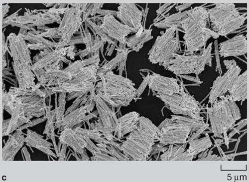
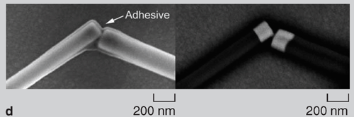
Any local roughness of the components (especially when the size approaches 100 nm) reduces the effective binding contact area due to asperities, and consequently decreases the strength and extent of binding. Hence, assemblies often consist of only a few bonded nanocomponents, and large-scale integration is not possible. It should be noted that in biological self-assembly, most of the components utilized in the assemblies are soft and deformable. This allows the mating surfaces to conform to one another, resulting in large contact areas for optimum binding. This study demonstrated the fabrication of 2-D and 3-D structures composed of rod-shaped metallic nanocomponents (referred to as nanowires) that were bonded to each other and to substrates using a curable adhesive or solder. Liquid layers of an organic adhesive or molten solder on specific regions of the nanowire facilitated binding between components. The adhesive and solder were subsequently hardened by curing (polymerization) and cooling, respectively. In the case of the adhesive, the 2-D and 3-D structures formed survived mild sonication and could be taken out of the fluidic medium without disruption. In the case of solder, it was possible to form ohmic low-resistance contacts that point to the feasibility of using these joints as nanoscale electrical contacts. FABRICATION AND SURFACE ENGINEERING OF NANOWIRES The use of nanowires as components for directed assembly was motivated by the fact that, in a relatively straight forward manner, large numbers of patterned nanowires could be fabricated ranging in diameter from 30200 nm and with lengths up to 20 µm.1517 Electrodeposition in nanoporous alumina or polycarbonate membranes (Figure 1a) was used to fabricate approximately 108109 nanowires (per membrane, Figure 1b). First, a thin seed layer of metal was evaporated on one side of the membrane to seal the pores. Electrodeposition of the wire was carried out sequentially using different electrolytes to pattern the wire with different metals along its length (Figure 1c). Since the nanowire contained different segments, it was possible to selectively functionalize parts of the wire using organic molecular self assembly (Figure 1d).35,36 Although the results in this article describe the use of metallic nanowires, the same strategy can be used to fabricate nanowires containing semiconducting and insulating segments15,16,37 to build electronically functional nanocomponents such as diodes or transistors.37,38
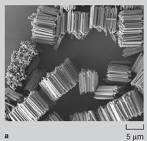
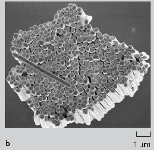
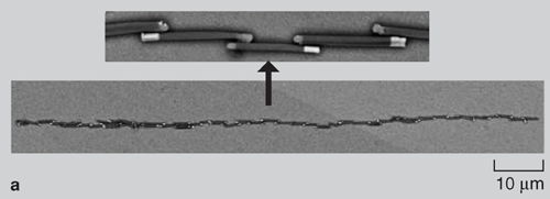
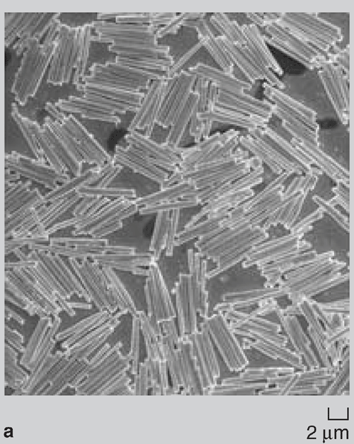
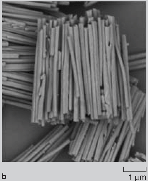
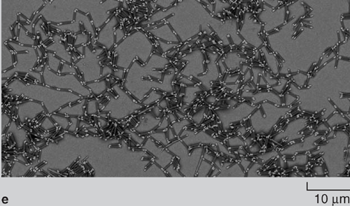
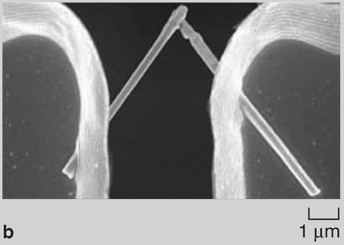
Since the surface-area-to-volume ratio of nanowires is high, there was a natural tendency of the wires to adhere to one another due to van der Waals forces. During dissolution of the nanoporous membrane containing gold wires, large bundle-like structures were observed (Figure 2a and 2b). Although these bundles are well ordered, they break apart readily on sonication and hence are of limited use in real-world applications. Directed Assembly of Nanowires When nanowires patterned with hydrophobic liquid layers collided with one another in a hydrophilic liquid, there was a tendency of the liquid layers on different nanowires to fuse with one another on contact in order to minimize their surface free energy. This surface tension force between liquid layers on colliding nanowires was large enough to hold the wires together in the liquid. Since this assembly involved binding between liquid layers (that were soft and deformable) patterned on the nanowires, the roughness of the wires did not hamper binding and it was possible to get large-scale integration. The magnetic-force-based assembly of nanowires was relatively straightforward.2830 When nanowires containing nickel segments (nickel segment length >> wire diameter) were tumbled in a magnetic field they bound to one another and aligned in the direction of the magnetic field (Figure 3a). The assembly of segmented nickel nanowires was also directed on patterned nickel substrates in magnetic fields. The wires aligned between nickel pads and the number of wires between adjacent pads could be controlled to some extent by controlling the nickel pattern on the substrate, the nanowire concentration, and the strength of the magnetic field (Figure 3b and 3c). Although the nanowires could be positioned on the patterned contact pads using magnetic fields, the nanowires were not strongly bound and were disrupted by mild sonication on removal from the magnetic field. Forming Bonded Nanowire
Structures This allowed segments to be selectively patterned on the same nanowire to be either hydrophobic (gold segment) or hydrophilic (nickel segment). To facilitate self-assembly, a small drop of a dilute solution of a hydrophobic polymerizable adhesive that was composed of a monomer (lauryl methacrylate), a crosslinker (1,6-hexanediol diacrylate), and a polymerization initiator (either a thermal initiator benzoyl peroxide or a photo-initiator, benzoin isobutyl ether) was introduced into a vial containing nanowires in ethanol. When water was added to the nanowire-adhesive-ethanol suspension, the hydrophobic adhesive preferentially precipitated on the hydrophobic gold segments.
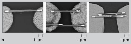
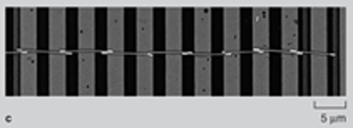
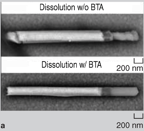
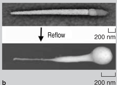
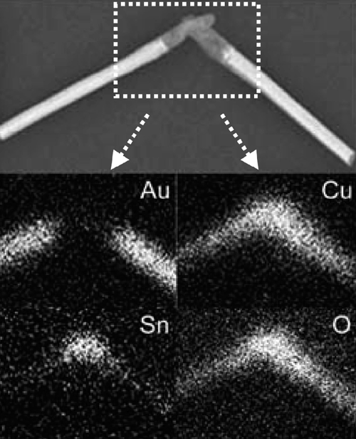
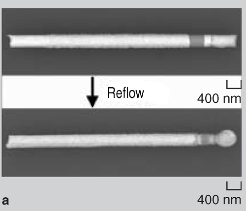
On agitation, the nanowires (with gold segments coated with adhesive) aggregated. Depending on how the assembly was carried out, either 2-D assemblies were obtained at the water-air interface or 3-D assemblies were obtained in the bulk. After the assembly, the monomeric adhesive was cured (polymerized) using ultraviolet light or heat to harden the adhesive and bond the assemblies. Structures with different topologies were fabricated using this methodology: 2-D rafts and 3-D bundles with pure gold wires (Figure 4a, b, and c) and 2-D Au-Ni-Au networks with predominantly end-to-end connectivity between gold segments (Figure 4d and e).39 On polymerization of the adhesive, the self-assembled aggregates formed were mechanically bonded and survived mild sonication. Nanowires were also soldered to one another and to substrates by either incorporating a solder segment within the nanowire itself or by directing the assembly of nanowires on substrates that were coated with a thin film (100 nm) of solder. Tin/lead (Sn/Pb, most widely used) solder or tin (a model lead-free solder) solder were deposited electrolytically. Unlike macroscopic soldering, since the solder volume present on the nanowires or substrate was very small it was crucial to protect the nanosolder surface from corrosion, intermetallic diffusion, and oxidation. During dissolution of the membrane in NaOH, the tin solder segments were readily corroded (Figure 5a). To minimize corrosion, a small quantity of the organic molecule benzatriazole (BTA) was added to the solution during membrane dissolution. The adsorption of BTA molecules on the surface of the nanowire protected the nanowire during dissolution and significantly improved corrosion resistance (Figure 5a). The impact of intermetallic diffusion was dramatic in nanowires that contained gold segments directly in contact with tin solder segments (Figure 5b). In this case, on heating above the melting point of the solder (reflow), the intermetallic diffusion between gold and tin was very dramatic as gold diffuses rapidly into tin. This intermetallic diffusion was minimized for optimum solder bonding by including a nickel spacer segment between the gold contacts and the tin solder.40 Any oxidation of the solder during reflow greatly reduces electrical conductivity of the joint formed. In these experiments, special care was taken to reduce oxidation during reflow using a tube furnace that was purged with nitrogen before, during, and after reflow. In the presence of air, the solder joint was extensively oxidized and it was difficult to form ohmic low-resistance electrical contacts. Figure 5c shows scanning-electron microscopy (SEM) energy-dispersive spectroscopy (EDS) maps of one such oxidized joint at room temperature after solder reflow, showing a large presence of oxygen in the joint region. Au-Ni-Au-Sn nanowires containing tin solder segments built into the wire were soldered (Figure 6a). A drop of a suspension of wires in ethanol was placed on a substrate and allowed to evaporate. Upon evaporation, the wires tended to aggregate at the edges of the drop and several wires lay near one another. When a silicon chip containing a high density of wires was heated in the tube furnace, the solder from adjacent wires lying next to one another fused into one another to form solder joints. On cooling, some of the wires were soldered to each other. To electrically characterize the solder joints, contact pads were lithographically aligned at the ends of the solder-bonded wires (Figure 6b).40 Current-voltage curves of the solder joints were measured, and it was observed that it was possible to form low-resistance ohmic solder joints. The measured resistances of soldered nanowires were in the range of 30200 Ω for 200 nm diameter wires.40 Au-Ni-Au nanowires were soldered onto nickel contact pads (on an oxidecoated silicon chip) that were covered with a thin layer of copper and Sn/Pb solder (solder ~100 nm thick). Nanowires used were composed of ferromagnetic nickel central segments terminated with gold contacts.41 The wires were first positioned on patterned nickel contact pads using magnetic fields as described earlier. After assembly, the wires were heated in a tube furnace in the presence of a nitrogen gas purge. The solder reflowed and bonded the nanowires to the contact pads (Figure 6c). The resistance between nanowire bridged contact pads dropped from 300106 Ω before reflow to about 13 Ω after reflow (for 200 nm diameter wires), indicating the formation of solder contacts with good electrical conductivity.41 This study demonstrated that it is possible to bond nanowires to one another and to substrates using adhesives or solder. The strategies outlined can be extended to other nanocomponents to form mechanically stable assemblies fabricated from the bottom up. It is also possible to use adhesive or solder bonding as a final step in the directed assembly of nanocomponents assembled by other forces such as molecular recognition or electrostatic forces. The authors believe that these strategies of forming mechanical and in some cases electrically conductive bonds between nanocomponents will find utility in nanomanufacturing and in developing structures engineered from the bottom up for use in real-world applications. ACKNOWLEDGEMENTS We acknowledge financial support from the National Science Foundation (CAREER/NSF-DMII) and the American Chemical Society Petroleum Research Fund. We thank Dr. Kenneth Livi for assistance with SEM EDS element analysis. REFERENCES 1. S.I. Stupp et al., Science, 276 (1997), pp. 384389. Zhiyong Gu (postdoctoral fellow), Hongke Ye (postdoctoral fellow), and David H. Gracias (assistant professor) are with the Department of Chemical and Biomolecular Engineering at Johns Hopkins University in Baltimore, Maryland. David Gracias is also with the Department of Chemistry at Johns Hopkins University. For more information, contact David H. Gracias, Department of Chemical and Biomolecular Engineering and Department of Chemistry, Johns Hopkins University, 3400 N. Charles Street, Baltimore, MD 21218; (410) 516-5284, fax: (410) 516-5510, e-mail: dgracias@jhu.edu.
|