More efficient and higher performance
photovoltaic solar cells continue to be
developed for spacecraft power and are
beginning to be developed for terrestrial
concentrators. The need for high-efficiency
and low-cost solar cells drives
research into new materials and new
materials applications. An overview of
active areas of research into high-performance
solar cells is presented in this
article.
INTRODUCTION
Next year (2008) will mark the 50-year
anniversary of the first practical use of
solar cells. Silicon solar cells provided
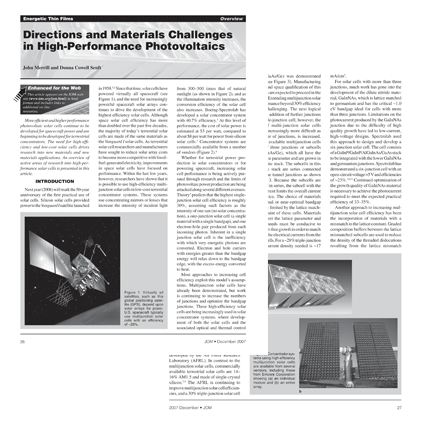
power to the Vanguard I satellite launched in 1958.1,2 Since that time, solar cells have
powered virtually all spacecraft (see
Figure 1), and the need for increasingly
powerful spacecraft solar arrays continues
to drive the development of the
highest efficiency solar cells. Although
space solar cell efficiency has more
than doubled over the past five decades,
the majority of todays terrestrial solar
cells are made of the same materials as
the Vanguard I solar cells. As terrestrial
solar cell researchers and manufacturers
have sought to reduce solar array costs
to become more competitive with fossil-fuel-generated electricity, improvements
in space solar cells have focused on
performance. Within the last few years,
however, researchers have shown that it
is possible to use high-efficiency multijunction
solar cells in low-cost terrestrial
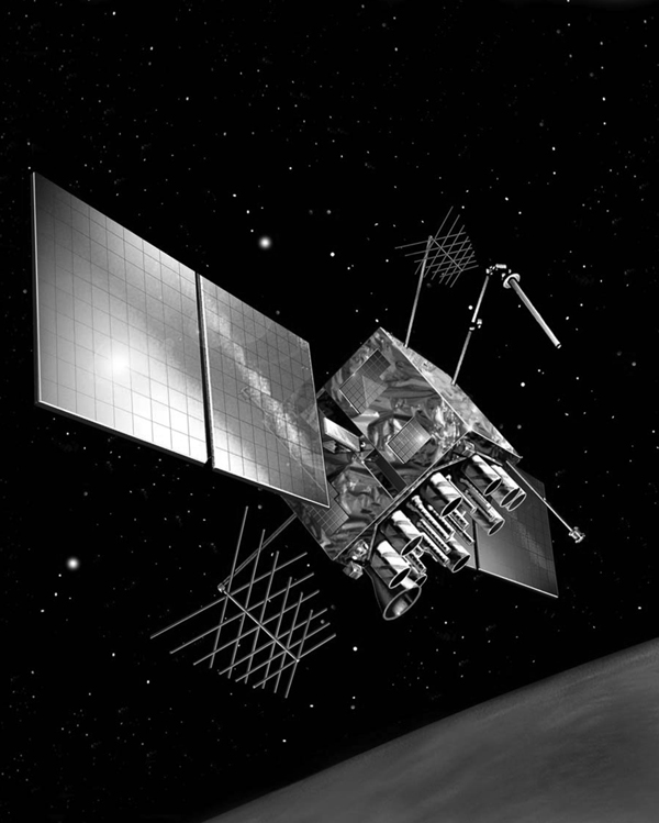
concentrator systems. These systems
use concentrating mirrors or lenses that
increase the intensity of incident light
from 300500 times that of natural
sunlight (as shown in Figure 2), and as
the illumination intensity increases, the
conversion efficiency of the solar cell
also increases. Boeing-Spectrolab has
developed a solar concentrator system
with 40.7% efficiency.3 At this level of
performance, the cost of solar power is
estimated at $3 per watt, compared to
about $8 per watt for power from silicon
solar cells.3 Concentrator systems are
commercially available from a number
of vendors (Figure 2).4
Whether for terrestrial power production
in solar concentrators or for
powering spacecraft, increasing solar
cell performance is being actively pursued
through research and the limits of
photovoltaic power production are being
attacked along several different avenues.
Theory5 predicts that the highest single-junction
solar cell efficiency is roughly
30%, assuming such factors as the
intensity of one sun (no solar concentration),
a one-junction solar cell (a single
material with a single bandgap), and one
electron-hole pair produced from each
incoming photon. Inherent in a single
junction solar cell is the inefficiency
with which very energetic photons are
converted. Electron and hole carriers
with energies greater than the bandgap
energy will relax down to the bandgap
edge, with the excess energy converted
to heat.
Most approaches to increasing cell
efficiency exploit this models assumptions.
Multijunction solar cells have
already been demonstrated, but work
is continuing to increase the numbers
of junctions and optimize the bandgap
junctions. These high-efficiency solar
cells are being increasingly used in solar
concentrator systems, where development
of both the solar cells and the
associated optical and thermal control elements are actively being pursued. Performance is also being advanced through the development of thin-film solar cells, where deposition of relatively low-efficiency solar cells on lightweight flexible substrates lead to high specific power (watts per array mass) and highly portable and stowable solar arrays. These arrays are highly advantageous for space and mobile terrestrial applications. On the forefront of research are solar cells that incorporate materials that produce more than one electron hole carrier per incoming photon and that incorporate nanotechnology. Photovoltaics research is a truly interdisciplinary field, involving
the fields of materials science, device physics, power engineering, and optics.
One point of confusion about solar cell efficiency should be mentioned. The measured efficiency of a solar cell depends on the spectrum of its light source. The space solar spectrum or air mass zero (AM0) spectrum is richer in ultraviolet light than the typical terrestrial
solar spectrum (air mass 1.5 or AM1.5).6 The ultraviolet light is typically converted into electrical power less efficiently
than other parts of the spectrum, resulting in lower AM0 efficiencies. For example, production multijunction solar cells are currently ~28% AM0, but these cells are over 32% efficient in the AM1.5 spectrum.7 Since cells are typically measured under the spectrum for their intended use and efficiencies are not easily converted, this article will indicate AM0 efficiencies unless otherwise specified.
MULTIJUNCTION SOLAR CELLS
Multijunction solar cells, commercially
available from Emcore (Albuquerque,
New Mexico) and Spectrolab (Sylmar, California), are comprised of III-V group materials stacked to form three photovoltaic junctions.8 This type of solar cell holds the record for the highest solar cell efficiency and was developed by the Air Force Research Laboratory (AFRL). In contrast to the multijunction solar cells, commercially available terrestrial solar cells are 1416% AM1.5 and made of single-crystal silicon.7,9 The AFRL is continuing to improve multijunction solar cell efficiencies,
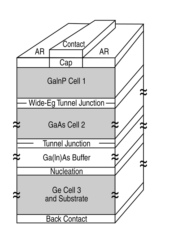
and a 30% triple-junction solar cell (GaInP2/GaAs/Ge) was demonstrated in 2003 (see Figure 3). Manufacturing scale-up and space qualification of this cell design are expected to proceed in the near term. Extending multijunction solar cell performance beyond 30% efficiency remains challenging. The next logical step is the addition of further junctions to the triple-junction cell; however, the growth of multi-junction solar cells becomes increasingly more difficult as the number of junctions, is increased. Currently available multijunction cells consist of three junctions or subcells (GaInP/GaAs/Ge), which all have the same lattice parameter and are grown in a monolithic stack. The subcells in this monolithic stack are series connected through the tunnel junctions as shown in Figure 3. Because the subcells are connected in series, the subcell with the lowest current limits the overall current of the device. The choice of materials with optimal or near-optimal bandgap is severely limited by the lattice matching
constraint of these cells. Materials that do meet the lattice parameter and bandgap needs must be conducive to near-defect-free growth in order to match or exceed the electrical currents from the other subcells. For a ~28% triple-junction cell, the current density needed is ~17 mA/cm2.
For solar cells with more than three junctions, much work has gone into the development of the dilute nitride material,
GaInNAs, which is lattice matched to germanium and has the critical ~1.0 eV bandgap ideal for cells with more than three junctions. Limitations on the photocurrent produced by the GaInNAs junction due to the difficulty of high quality growth have led to low-current, high-voltage designs. Spectrolab used this approach to design and develop a six-junction solar cell. The cell consists of a GaInP/GaInP/AlGaInAs/GaAs stack to be integrated with the lower GaInNAs and germanium junctions. Spectrolab has demonstrated a six-junction cell with an open-circuit voltage >5 V and efficiencies of ~23%.10,11 Continued optimization of the growth quality of GaInNAs material is necessary to achieve the photocurrent required to meet the expected practical efficiency of 3335%.
Another approach to increasing multijunction
solar cell efficiency has been the incorporation of materials with a mismatch in the lattice constant. Graded composition buffers between the lattice mismatched subcells are used to reduce the density of the threaded dislocations resulting from the lattice mismatch strain. Lattice mismatch technology opens the parameter space for junction materials, allowing the choice of materials
with more optimal bandgaps and a potential for higher cell efficiency. Spectrolab (under an AFRL contract) has demonstrated a 28.8% efficient three-junction (GaInP/GaInAs/Ge) solar cell incorporating 0.5% mismatch in the lattice constant.12
Despite the success identified here, the conventional lattice mismatch approach can suffer from a number of problems including high defect density,
rough surface morphologies, and epilayer cracking/bowing and has not yet produced efficiencies greater than that achieved from a lattice matched triple-junction cell. Because the buffer layer is grown prior to the high bandgap subcells, defects can propagate into these subcells, limiting the quality of the material
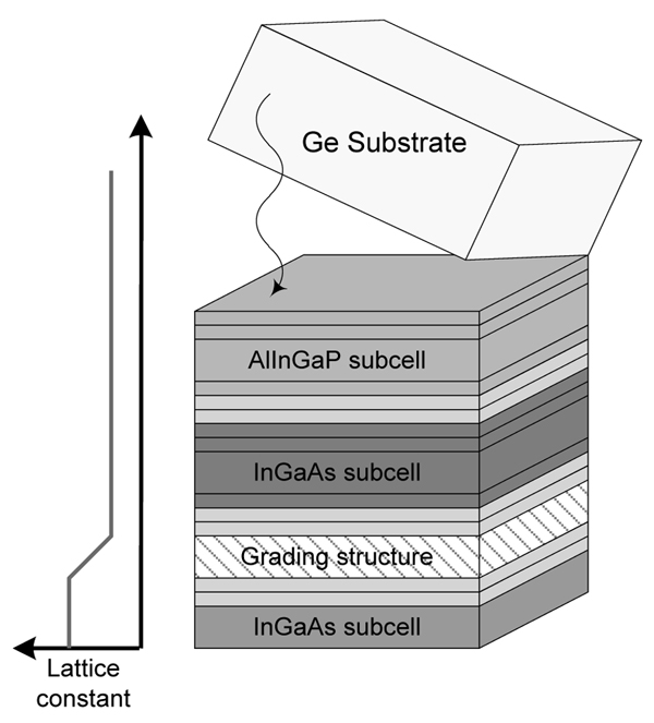
and thus the efficiency. To overcome these limitations, M.K. Wanlass et al.13 from the National Renewable Energy Laboratory proposed a novel concept, now often referred to as an inverted metamorphic structure (IMM), in which the mid- and high-bandgap subcells are grown lattice matched to a germanium or GaAs substrate. A buffer layer is then grown followed by a lower bandgap material. The device is then mounted to a surrogate substrate and the parent substrate removed. In this way, the lattice-matched higher bandgap subcells are grown first and should be of high quality. Because the higher bandgap subcells produce a larger percentage of the power, this cell structure has the potential for higher efficiencies than the conventional lattice-mismatched cell. Additionally, because the thick germanium substrate must be removed, the cell can be significantly lower in mass and can be flexible. Emcore, under an AFRL program, has demonstrated a small-area cell based on this type structure
at 31.9% efficiency.14 A depiction of this cell structure is shown in Figure 4. This structure is expected to reach a practical efficiency of 33% in large area manufacturable solar cells in the next several years. Similar approaches for more than three junctions grown inverted have the potential of reaching efficiencies of 35% or greater.
Wafer bonding is a technique that is in wide use today to manufacture silicon-on-insulator (SOI) wafers, light-emitting diodes (LEDs), and other optoelectronic devices, and had its first applications in the 1980s.15 The SOI wafer bonding application is more prevalent, but optoelectronic
devices use the same III-V materials found in multijunction solar cells. Despite the materials similarities, the technique has not until recently been applied to solar cells. Wafer bonding is a current area of research for improving the efficiency of multijunction solar cells. The attraction is that junction materials may be physically stacked and bonded, chosen for their bandgaps in order to optimize the efficiency of the solar cell. The materials choice of III-V compounds is currently limited by lattice parameter, so that the materials can be grown monolithically by metal organic chemical vapor deposition.
The need to avoid defects that serve as carrier recombination sites imposes a new level of perfection on established wafer bonding techniques, although the basic process is the same for bonding all wafers. The first step is to mirror polish the wafer surfaces, followed by bringing
the surfaces into contact in a clean environment.15 After room-temperature bonding, the wafers are annealed at a higher temperature to improve the strength of the bond. One of the bonded wafers can be thinned by polishing, chemical etching, or plasma etching. The smart-cut method allows the bulk of the original wafer to be removed through a controlled fracture induced by hydrogen implantation and microcracking.15 With any of these methods, the result is a transfer of a thin layer of single-crystal material onto a foreign substrate. Several factors can result in imperfect bonding. Particles or surface imperfections of 1 μm are sufficient to cause interface bubbles where no bonding occurs. Evolution of hydrogen gas at the interface can also cause unbonded regions. Problems with bonding strength and interface bubbles tend to be minimal for a hydrophilic surface
(such as silicon oxide) bonding with a hydrophobic surface (such as a silicon wafer) but are greater for the bonding of two hydrophobic III-V surfaces.15
The quality of electrical conductivity
across the interface and the level of defects imposed by the wafer bonding process are only acceptable if the bonded layer is inserted into the tunnel junction portion of the multijunction solar cell (see Figure 3). GaAs/InGaAs wafer-bonded solar cells have been demonstrated and reported in the literature.16,17 Devices so far are < 1 cm2, and one of the challenges to making this a commercial technology will be scaling to larger area devices.
HIGH-PERFORMANCE
THIN-FILM SOLAR CELLS
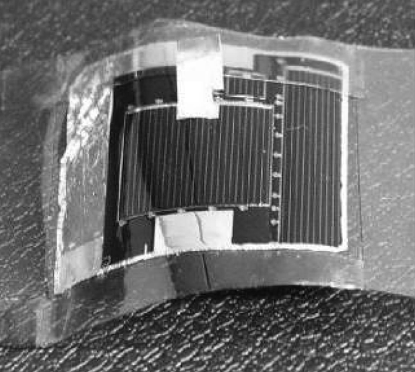
Next-generation thin-film solar arrays, because of their increased specific power, inherent radiation hardness, and high stowage efficiency, are of interest for space applications. Because of the potential
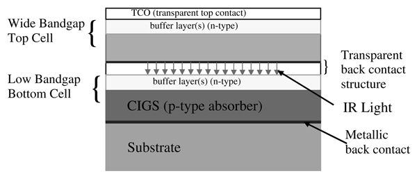
for low-cost production, significant research has gone into developing low-cost thin-film solar cells for the terrestrial market. Thin-film solar cells have been primarily based on Cu(In,Ga)Se2 (also called CIGS), amorphous silicon, or CdTe alloys. Application of these technologies
for use in space has been, and continues to be, the stronger driver for developing higher performance both in terms of specific power and efficiency. Products with high specific power are now transitioning to use, but the desired higher efficiency has not been fully achieved.
Production amorphous silicon (a-Si) solar cells are available from United Solar Ovonic on polyimide with efficiencies as high as 9.6% and cell-level specific power >2,300 W/kg when monolithically integrated. The cell is a triple-junction stack based on a-Si and a-SiGe alloys. The incorporation of nanocrystalline silicon (nc-Si) into one of the a-SiGe-containing subcells shows promise for higher efficiencies, as well as less susceptibility to light degradation that is normally seen in a-Si cells. United Solar Ovonic has demonstrated 12.6% efficiency in small area cells incorporating
nc-Si. However, challenges remain in deposition of high-quality nc-Si at rates high enough to be manufacturable.18
NANO-ENHANCED
SOLAR CELLS
The quest for application of nanotechnologies
has led to a myriad of concepts being pursued to take advantage of size-dependant spectral absorption in seeking higher-efficiency solar cells. Conceptually,
the most straightforward approach is combining nanoparticles of different sizes in a device to absorb the entire solar spectrum. An example is a nanocomposite
solar cell, fabricated by embedding nanostructures in a conjugated polymer matrix. To date these devices have shown low efficiencies, mainly due to poor hole mobility in the polymer matrix, and they degrade quickly. Another approach is the concept of an intermediate bandgap solar cell. In this approach, nanostructures
are introduced into a material, creating bands in the solar cell at energies other than the physical bandgap of the solar cell. The added energy levels create additional absorption mechanisms in the cell, which theoretically can be optimized
to increase solar absorption. In the case of an intermediate bandgap cell, nanoparticles can be added to fine-tune the bandgap of a solar cell or subcell. For example, a quantum dot array could be added to a subcell of a III-V triple-junction solar cell to create a more optimal bandgap. The modified bandgap allows more efficient absorption of the spectrum and better current matching through the cell, leading to higher efficiency.
The challenge is to balance the incorporation of enough quantum dots in the depletion region to get increased current against the potential for decreased material quality and lower minority carrier
diffusion lengths. To date, fabricated cells have not demonstrated higher efficiency
than non-quantum-dot containing control samples, although promising research continues. However, the approach also has promise in increased radiation hardness and better temperature coefficients;21 recently presented results have demonstrated this potential.22,23
Another nanotechnology-based method of increasing solar cell efficiency is carrier multiplication, increasing the number of electron-hole charge carriers (excitons) produced for each incoming photon. M.C. Hanna and A.J. Nozik24 calculate that the theoretical efficiency of a single-junction solar cell increases from 33.7% to 41.9% if carrier multiplication
of up to a factor of 2 is allowed. In this case, two excitons are produced for incoming photons of energy Ei, where Ei > 2Eg. (Eg is the energy gap of the solar cell material.) If carrier multiplication
increases to a maximum of 6, the theoretical efficiency becomes 44.4%. R.D. Schaller et al.25 have experimentally shown a carrier multiplication factor of 7 in PbSe nanoparticles. Carrier multiplication
is enhanced in nanoparticles as compared to bulk materials due to conservation
of energy and momentum and carrier confinement in nanoparticles.26 Photovoltaics using carrier multiplication
would be especially advantageous for space applications due to the high energy photons in the space solar spectrum
that are screened out from the earths atmosphere. The main challenge to implementing high-efficiency carrier multiplication is in extracting the charges from the nanoparticles as discussed by V.I. Klimov.27 Other challenges discussed by Klimov concern the conductivity and surface chemical stability of the nanoparticles.
Undoubtedly, the challenge of integrating nanoparticles into a workable solar cell device will be significant.
CONCLUSION
The search for higher-efficiency solar cells continues. These cells are needed to reduce the size and mass for satellite power systems and to provide cost-competitive
terrestrial power in concentrator systems. Triple-junction solar cells based on III-V semiconductors have shown that a market exists for both of these applications, and the need for further advancements exists. Promising research avenues are in nanotechnology, wafer bonding, and lattice mismatch growth, while the concept of composite nanodot solar cells remains largely unfulfilled. Prospects for increasing the efficiencies of flexible thin-film solar cells through two-junction approaches are good. As the commercial market for terrestrial concentrator systems grows, it will be interesting to note whether the space market continues to drive the development
of high-efficiency solar cells or if the larger terrestrial market assumes the driving role. A great deal of attention has been given to theoretical efficiency calculations of novel types of solar cells, and now work on materials and processing methods is needed to fulfill these promises. A great deal of work in the materials area remains before solar cell performance can begin to approach theoretical limits.
REFERENCES
1. A.K. Hyder et al., Spacecraft Power Technologies, 1st ed. (London: Imperial College Press, 2000), p. 1.
2. Vanguard, A History (NASA SP-4202, 1970), online book, http://history.nasa.gov/SP-4202/toc.html.
3. New World Record Achieved in Solar Cell Technology,www.energy.gov/news/4503.htm.
4. G. Herring, Focused on Concentration, Photon Int. (July 2005), p. 50.
5. W. Shockley and H.J. Queisser, Detailed Balance Limit of Efficiency of p-n Junction Solar Cells, J. Appl. Phys., 32 (3) (1961), pp. 510519.
6. S.M. Sze, Physics of Semiconductor Devices, 2nd ed. (New York: John Wiley & Sons, 1981), pp. 791798.
7. M.A. Green et al., Solar Cell Efficiency Tables (Version 28), Prog. Photovolt: Res. Appl., 14 (2006), pp. 455461.
8. D.C. Senft, Progress in Crystalline Multijunction and Thin-Film Photovoltaics, J. Electronic Materials, 34 (5) (2005), pp. 571574.
9. R. Hezel, Progress in Manufacturable High-Efficiency Silicon Solar Cells, Advances in Solid State Physics Series, Vol. 44 (Springer, Berlin / Heidelberg, 2004).
10. R.R. King et al., Metamorphic III-V Materials, Sublattice Disorder, and Multijunction Solar Cell Approaches with over 37% Efficiency, Proc. 19th European-Photovoltaic Solar Energy Conf. (London: James & James, 2004), p. 3587.
11. R.R. King et al., Bandgap Engineering in High-Efficiency Multijunction Concentrator Cells, Proc. International Conference on Solar Concentrators for the Generation of Electricity or Hydrogen (Golden, CO: National Renewable Energy Lab, 2005), report # 20060007941.
12. D.C. Law et al., Multijunction Solar Cells with Subcell Materials Highly Lattice-Mismatched to Germanium Proceedings of the 31st IEEE Photovoltaic Specialists Conference (Piscataway, NJ: IEEE, 2005), pp. 575578.
13. M.W. Wanlass et al., Lattice-Mismatched Approaches for High-Performance, III-V Photovoltaic Energy Converters, Proceedings of the 31st IEEE Photovoltaic Specialists Conference (Piscataway, NJ: IEEE, 2005), pp. 530535.
14. P.R. Sharps et al., Surpassing the 30% Efficiency Level for Multijunction Space Solar Cells, (Paper presented at Space Power Workshop 2006, El Segundo, Ca, April 2006).
15. U. Gösele and Q.-Y. Tong, Semiconductor Wafer Bonding, Annu. Rev. Mater. Sci., 28 (1998), pp. 215241.
16. K. Tanabe et al., Direct-bonded GaAs/InGaAs Tandem Solar Cell, Appl. Phys. Lett., 89 (2006), p. 102106.
17. A. Fontcuberta et al., InGaAs/InP Double Heterostructures on InP/Si Templates Fabricated by Wafer Bonding and Hydrogen-Induced Exfoliation, App. Phys. Lett., 83 (26) (2003), pp. 54135415.
18. A. Banerjee et al., Thin Film Triple-Junction Amorphous Silicon Solar Cells and Modules on Polymer Substrate, (Paper presented at Space Power Workshop 2006, El Segundo, Ca, April 2006).
19. T. J. Coutts, K.A. Emery, and J.S. Ward, Modeled Performance of Polycrystalline Thin-Film Tandem Solar Cells, Progress in Photovoltaics, 10 (3) (2002), pp. 195203.
20. L.M. Woods et al., Wide-Bandgap CIAS Thin-Film Photovoltaics with Transparent Back Contacts for Next Generation Single and Multi-Junction Devices, Materials Science and Engineering B, 116 (2005), pp. 297302.
21. R.P. Raffaelle et al., Radiation Degradation of Nanomaterials, Materials Research Society Symposium Proceedings #887: Degradation Processes in Nanostructured Materials (Warrendale, PA: MRS, 2006), pp. 147157.
22. B.D. Weaver, B.J. Landi, and R.P. Raffaelle, High Radiation Tolerance of Carbon Nanotube Matrices for Space Power Applications, 2nd International Energy Conversion Engineering Conference Proceedings (Reston, VA: American Institute of Aeronautics and Astronautics, 2004), AIAA-2004-5530.
23. R.P. Raffaelle et al., Nanomaterials for Space Solar Power (Presentation at the Space Power Workshop 2007, El Segundo, CA, April 2007).
24. M.C. Hanna and A.J. Nozik, Solar Conversion Efficiency of Photovoltaic and Photoelectrolysis Cells with Carrier Multiplication Absorbers, J. of Appl. Phys., 100 (2006), p. 074510.
25. R.D. Schaller et al., Seven Excitons at a Cost of One: Redefining the Limits for Conversion Efficiency of Photons into Charge Carriers, Nano Lett., 6 (3) (2006), pp. 424429.
26. M. Califano, A. Zunger, and A. Franceschetti, Direct Carrier Multiplication Due to Inverse Auger Scattering in CdSe Quantum Dots, Appl. Phys. Lett., 84 (13) (2004), pp. 24092411.
27. V.I. Klimov, Mechanisms for Photogeneration and Recombination of Multiexcitons in Semiconductor Nanocrystals: Implications for Lasing and Solar Energy Conversion, J. Phys. Chem. B, 110 (2006), pp. 1682716845.
John Merrill and Donna Cowell Senft are with the Air Force Research Laboratory Space Vehicles Directorate, 355 3550 Aberdeen Ave SE, Kirtland AFB, NM 87122. Dr. Merrill can be reached at e-mail: AFRL.VSSV@kirtland.af.mil.
|
 Presenting a Web-Enhanced