 Presenting a Web-Enhanced Presenting a Web-Enhanced Article from JOM |
 LATEST ISSUE |
|||
TMS QUICK LINKS: |
• TECHNICAL QUESTIONS • NEWS ROOM • ABOUT TMS • SITE MAP • CONTACT US |
JOM QUICK LINKS: |
• COVER GALLERY • CLASSIFIED ADS • SUBJECT INDEXES • AUTHORS KIT • ADVERTISE |
|
| Research Summary | Vol. 60, No.4 p. 29-32 |
The Characterization of Various ZnO
Nanostructures
Using Field-Emission
SEM
Zhiyong Xu, Jiann-Yang Hwang, Bowen Li, Xiaodi Huang, and Howard Wang
Questions? Contact jom@tms.org. |

|
Zinc oxide (ZnO) is a unique material that has prompted a vast amount of research. Various morphologies and sizes of ZnO materials have led to a wide range of promising applications. Although research related to the applications of ZnO is progressing rapidly, it has been an enormous challenge to produce uniform ZnO materials. A unique synthesis method to produce ZnO materials with various morphologies has been studied and is presented in this paper. Field-emission scanning-electron microscopy has been utilized to characterize ZnO materials in this study to show how the synthesis conditions control the morphologies of ZnO.
Zinc oxide, a wide-band-gap semiconducting oxide, has attracted tremendous attention due to potential applications such as transparent conductive films, high-efficiency vacuum fluorescent displays, field-emission displays, solar-cell windows, and acoustic wave devices. In order to realize all these applications, it is crucial to devise simple and efficient methods for preparing ZnO on a large scale at low cost. A variety of ZnO nanostructures
have been fabricated using different
synthesis methods in recent years for
many promising applications. There
are many synthesis methods available
to produce ZnO nanostructures, including thermal evaporation of zinc oxide
powders (at 1,400°C),1 vapor-phase
transport processes,2,3 and solution synthesis.4-6 All these synthesis methods
have some disadvantages. Z. Ren et al.
have combined a general molten-salt
process to develop a new synthesis approach:
molten-salt-assisted thermal
evaporation.7 Materials used in this experiment include
zinc metal (in dust form), a surfactant,
sodium chloride, and platinum
metal (both wire and sheet form). Zinc
dust (~3-10 μm) was obtained from
Fisher Scientific and sodium chloride
was obtained from Fisher Chemicals.
The surfactant used was IGEPAL CO-
660, which contains ethoxylated nonylphenol
[C9H19C6H4(OCH2CH2)nOH]
and polyethylene glycol [H(OCH2CH2)nOH].
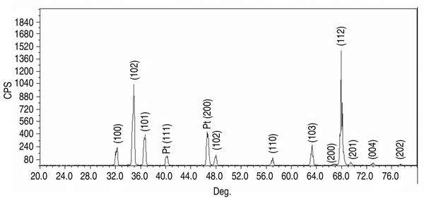
All samples had similar XRD patterns
with high crystallinity, even
though the ZnO samples have various
morphologies. Figure 1 shows a typical
XRD pattern of all the resulting samples.
The XRD diffraction peaks can be
indexed as wurtzite (ZnO) having a
hexagonal structure (space group
C6mc) with lattice parameters a =
3.2496 Å and c = 5.2065 Å (JCPDS
Card No. 36-1451). Only peaks from
wurtzite and platinum (from platinum
wire or sheet) were detected.
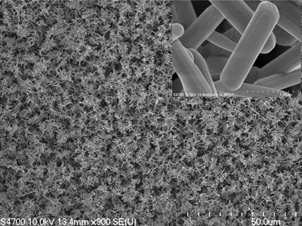
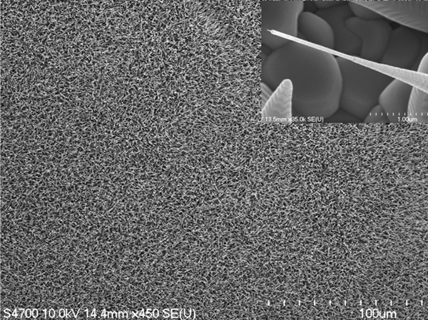
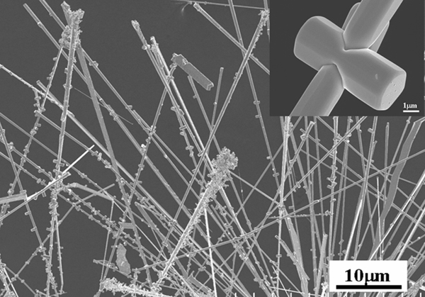
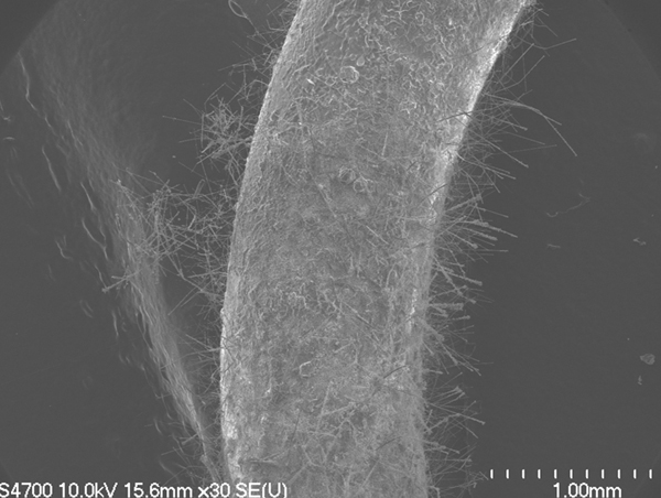
A typical FESEM image for ZnO
grown on platinum sheet from R2 is
shown in Figure 3. This image shows
that a very high yield of uniform needle-like ZnO nanostructures (with
sharp ends) was formed on the platinum
substrate. After this critical point, the temperature
in the crucible rose rapidly from
burning the organic matter in the crucible.
Zinc started to form zinc vapor,
which reacted with platinum (whose
temperature was still the same as the
furnace chamber) and air to form a
ZnO particle layer first (shown in Figure
3). As the temperature of the furnace
chamber rose, crystalline ZnO
began to grow on top of the previously
formed ZnO particle layer. The concentration
of zinc gradually decreased
and this led to the formation of needle-shaped
ZnO particles shown in Figure
3. This indicates that controlling the
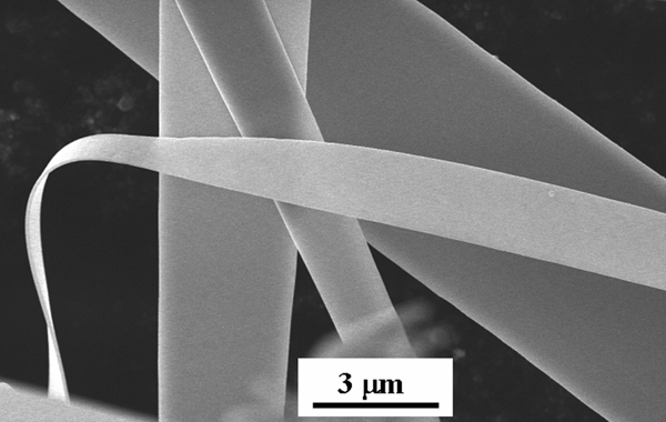
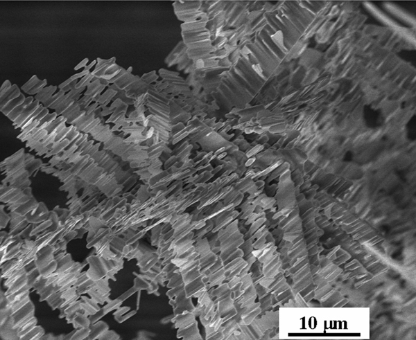
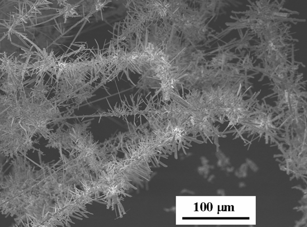
heating process will provide a means of
controlling the final ZnO morphology. Various ZnO nanostructures can be obtained by changing the thermal routes for combustion synthesis of ZnO and the geometries of substrates. These thermal changes and varying substrates might provide a means of controlling ZnO. Field-emission scanning-electron microscope imaging has been a necessary tool for determining morphologies of the ZnO structures, which is a key component to the usefulness of ZnO materials. Typically, various ZnO structures have the same crystalline structure. The morphology of ZnO is a key factor in differences in their properties. Many applications of ZnO nanostructures have been identified due to their morphological dependence. For example, the luminescence property of ZnO is morphology-dependent. The relative intensity of luminescence is greatest for nanowire and least for nano-particle (nanowire > powder > nano-needle > nano-particle).8 Field-emission scanning- electron microscopy, therefore, as a powerful image analyzer, is very useful for studying various ZnO nanomaterials morphologies. Support from the U.S. Department of Energy under the Hydrogen Storage Program Grant number DE-PS36- 03GO93013, is greatly appreciated. REFERENCES 1. Z.W. Pan, Z.R. Dai, and Z.L. Wang, Science, 291 (2001), p. 1947. 2. M.H. Huang et al., Adv. Mater, 13 (2001), p. 113. 3. M.H. Huang et al., Science, 292 (2001), p. 1897. 4. L. Vayssieres et al., J. Phys. Chem. , 105 (2001), p. 3350. 5. L. Vayssieres et al., Chem. Mater., 13 (2001), p. 4395. 6. L. Vayssieres, Adv. Mater, 15 (2003), p. 464. 7. Z. Wang et al., Adv. Mater, 18 (2006), p. 3275. 8. X.H. Sun et al., J. Phys. Chem. B, 109 (2005), p. 3120. Zhiyong Xu, Jiann-Yang Hwang, Bowen Li, and Xiaodi Huang are with the Institute of Materials Processing and Department of Materials Science and Engineering, Michigan Technological University, Houghton, MI 49931; Howard Wang is with the Department of Mechanical Engineering, Binghamton University, Binghamton, NY 13902-6000. Dr. Hwang can be reached at (906) 487-2600; e-mail jhwang@mtu.edu. |