|
|
|
June 22-24 • Santa Barbara, California
|
|
|
| SAMPLE ABSTRACTS
|
|
View the presentation, "Effect of Carbonization Process Conditions on Surface Morphology of 3C-SiC Films Grown on Si Substrates" as a sample abstract
and extended abstract.
|
|
EMC 2011: Technical Program
June 22-24, 2011 • University of California • Santa Barbara, CA
The EMC 2011 technical program session sheets are now available
online or download the
Final Program (PDF). All sessions will be held on the campus of the University of California - Santa Barbara. The technical program commences with the EMC Student Awards Ceremony and Plenary Lecture on Wednesday at 8:20 a.m.
PROCEEDINGS
Conference Proceedings
New In 2011! All EMC authors will have the opportunity to be published in a special edition of The Journal of Electronic Materials (JEM), which will feature collected papers from the entire Electronic Materials Conference 2011. Manuscripts will be accepted from June 15, 2011 to August 1, 2011.
Visit the EMC Proceedings page for submission guidelines and instructions.
EMC 2011 PLENARY SPEAKER
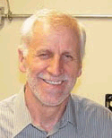
Plenary Speaker: Wladek Walukiewicz
Wladek Walukiewicz, senior staff scientist, Lawrence Berkeley National Laboratory, will present "New Concepts and Materials for Solar Energy Conversion" on Wednesday, June 21, 8:30 a.m. Corwin Pavilion
Efficient conversion of solar photons into other forms of energy has become one of the primary objectives of the modern science and technology. In the presentation, Walukiewicz will briefly review the various large scale energy related research projects at Berkeley. The core presentation will focus on methods to engineer the energy band structure of semiconductor materials for specific energy related applications. He will discuss recent progress on applications of group III-nitride semiconductor alloys for full solar spectrum, high efficiency multi-junction solar cells. The second part of the presentation will focus on the recent advances in using highly mismatched semiconductor alloys for intermediate band solar cells. Walukiewicz will offer the most recent results on demonstration of the first intermediate band photovoltaic device. Finally, he will discuss potential applications of the highly mismatched alloys for the photoelectrochemical solar water splitting.
Walukiewicz's presentation was developed in collaboration with the Solar Energy Research Group and is supported by the Division of Materials Science and Engineering, U.S. Department of Energy.
TECHNICAL TOPICS
Authors may submit papers on the following symposia topics. Each technical area
is being organized by a committee. Visit the organizers page for a list of the organizers' names.
Energy Conversion and Storage Materials
- Photovoltaics: Organic and Hybrid
- Highly Mismatchd Dilute Alloys
- Next Generation Solar Cell Materials and Devices
- Thermoelectrics and Thermionics
- Ionic Conductors for Solid Oxide Fuel Cells and Batteries
Issues for Wide Bandgap Materials
- Group III-Nitrides: Growth, Processing, Characterization, Theory and Devices
- UV Detectors and Emitters: Materials and Devices
- Silicon Carbide: Growth, Processing, Characterization, Theory and Devices
- Oxide Semiconductors: Growth, Doping, Defects, Nanostructures and Devices
- Indium Nitride: Growth, Processing, Characterization, Theory and Devices
- Point Defects, Doping and Extended Defects
Nanoscale Science and Technology in Materials
- Graphene and Carbon Nanotubes
- Nanotubes and Nanowires
- Low-Dimensional Structures: Quantum Dots, Wires and Wells
- Nanoscale Characterization: Scanning Probes, Electron Microscopy and Other Techniques
- Molecular Electronics: Devices, Materials and Sensors
Enabling Technologies
- Metamaterials
- Flexible and Printed Thin Film Electronics
- Organic Thin Film and Crystalline Transistors: Devices, Materials and Processing
- Nano-Magnetic, Magnetic Memory and Spintronic Materials
- Contacts to Semiconductor Epilayers, Nanowires, Nanotubes and Organic Films
- Epitaxial Materials and Devices
- Narrow Bandgap Materials and Devices
- Nondestructive Testing and In Situ Monitoring and Control
- Semiconductor Processing: Oxidation, Passivation, and Etching
- Materials Integration: Wafer Bonding and Engineered Substrates
- Oxide Thin Film Integration: Alternative Dielectrics, Epitaxial Oxides, Multifunctional Oxides, Superlattices and Metal Gates
- Si-Based Heterojunctions
- Compound Semiconductor Growth on Si Substrates (Heteroepi on Si)
FOR MORE INFO...
For more information about this meeting, please complete the meeting inquiry form or contact:
TMS Meeting Services
184 Thorn Hill Road
Warrendale , PA 15086-7514 USA
Telephone (724) 776-9000, ext. 243
(800) 759-4TMS
Fax: (724) 776-3770
E-mail: mtgserv@tms.org
|