This article presents an overview of the
recent developments in the fundamental understandings and microelectronics
applications of metal silicides. The synthesis and characterization of nanoscale
silicides with potential applications in nanotechnology are reviewed.
INTRODUCTION
Metal silicide thin films are integral
parts of all microelectronics devices.
They have been used as ohmic contacts,
Schottky barrier contacts, gate electrodes,
local interconnects, and diffusion
barriers. With advances in semiconductor
device fabrication technology, the
shrinkage in line width continues at a
fast pace. The International Technology
Roadmap for Semiconductors
(ITRS) predicted that in 2005, in the 90
nm generation devices, the gate length
and thickness of silicide at the contact
window would be 32 nm and 20 nm,
respectively. In the year 2007, for the 65
nm generation devices, these numbers
are predicted to further decrease to 25
nm and 17 nm, respectively.1
|
"Interconnectors provide flexibility in circuit design and substantial reduction in die size, and, thus, chip cost. " |
|
In addition,
more transistors will be incorporated in
one chip. However, owing to the demand
for increased integration level, the surface
area will not be adequate to meet
the interconnect demand. Multi-level
interconnections provide flexibility in
circuit design and a substantial reduction
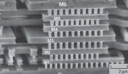
in die size and, thus, chip cost. Figure 1
shows a scanning electron microscope
(SEM) cross section of a six-level metal
backend structure. Electrical connection
between the various metal layers
is provided by vertical interconnects
commonly referred to as vias.
See the sidebar for device application
details.
|
DEVICE APPLICATIONS
|
For metallization of integrated circuit (IC) devices, transition metal silicides, including
near-noble and refractory metal silicides, are used. The general requirements are: low
resistivity; good adhesion to silicon; low contact resistance to silicon; appropriate
Schottky barrier height or Ohmic with heavily doped silicon (n+ or p+); thermal stability;
appropriate morphology for subsequent lithography and etching; high corrosion
resistance; oxidation resistance; good adhesion to and minimal reaction with SiO2; low
interface stress, compatible with other processing steps such as lithography and etching,
minimizing metal penetration; high electromigration resistance; and formability at low
temperature. The requirements are rather stringent and at present, only three silicides,
TiSi2, CoSi2, and NiSi, are being considered for metal contacts for advanced devices.2
PtSi and Pd2Si were used early on for metal contacts to lower the contact resistance
of aluminum alloys as well as to serve as a diffusion barrier layer between aluminum
alloy film and silicon. In the early 1980s, as the linewidth decreased to about 1 μm,
many refractory metal silicide films, such as MoSi2, WSi2, TiSi2, and TaSi2 were used by
different manufacturers. For the 0.25 μm technology, TiSi2 was almost used exclusively.3
For devices with linewidth of 0.18 µm or smaller, TiSi2, CoSi2, and NiSi are possible
candidate contact materials.4,5
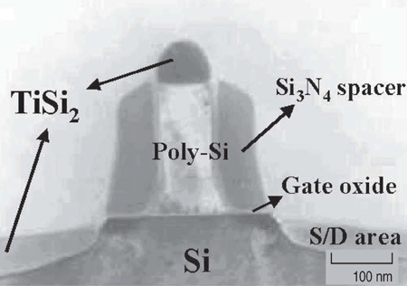
Many different deposition techniques can be used to deposit metal thin films. Currently,
sputtering is used almost exclusively to deposit metal layers for contacts or in the self-aligned
silicidation (salicide) process. Figure A shows a self-aligned TiSi2, which was
formed on source, drain, and gate simultaneously. On the other hand, chemical vapor
deposition of WSix and tungsten films is the dominant method to form gate electrodes or
local interconnects and metal plugs, respectively.
The usual steps to form a silicide begin with the cleaning of the wafers consecutively
by organic solution, dilute hydrochloric acid (HF), and deionized water. The wafers are
blown dry with a nitrogen gun or in a spin-rinse-dry process. An alternative is to dip
the wafer in dilute HF then blow dry with a nitrogen gun or spin dry. The wafers are
immediately placed in the metal deposition chamber and the surface is sputter-cleaned
by argon ions if necessary (argon sputtering may cause particle issue). Next, metal thin
films are deposited on silicon at room temperature or at a higher temperature, and finally,
the wafers are heat treated either by traditional furnace annealing or by rapid thermal
annealing to form silicides.
Prior to the deposition of metal thin films, a 1.5-nm to 2-nm-thick SiO2 layer was
usually present at the silicon substrate surface following the etching of the thermal oxide.
It is necessary for the contact metal layers to penetrate the thin oxide layer to react
with the silicon to form silicides. Titanium and nickel atoms are capable of penetrating
through the thin oxide. On the other hand, cobalt atoms have difficulty forming silicide
with silicon if a thin oxide layer is present at the interface. An argon ion sputter-cleaning
step is usually required. Since CoSi2 is widely used in devices with linewidths of 0.18 μm or smaller, the formation of CoSi2 is used as an example to illustrate the steps to
form silicides on silicon. The deposition of cobalt thin films by sputtering is kept at room
temperature. A mixture of Co2Si and CoSi is formed at 300°C. CoSi2 forms at 550°C.4
For rapid thermal annealing, the first-step and second-step annealings are conducted at
500550°C for 3060 s and 700850°C for 3060 s, respectively.
|
SILICIDE FORMATION
The impetus for the study of silicide
formation on silicon was stimulated
by the expectation of device applications
of silicides in the late 1970s and
early 1980s. Two review chapters have
succinctly summarized the knowledge
accumulated up to the early 1980s.6,7
This article focuses on the most important
developments in recent years.
Solid-State Amorphization
In device applications, interfacial
reactions of metal thin films with silicon
are rather peculiar in that polycrystalline
metal film reacts with single-crystal silicon.
The substrate is covalently bonded
and the thin film is metallic. As a result,
the microstructure of the silicide film and
orientation of the substrate may play an
important role in influencing the reaction.
Some silicides can form at a temperature
as low as 100°C. The mechanism for the
break up of silicon bonds at such a low
temperature is rather intriguing.7 Furthermore,
the silicide phases formed at
relatively low temperature are apparently
related more to the growth kinetics than
they are dictated by the thermodynamic
consideration.
The formation of an amorphous
interlayer (ainterlayer) by solid-state
diffusion in diffusion couples has been
one of the most challenging problems
in condensed matter physics in recent
years. The a-interlayer has been found
to occur in all refractory metal/silicon
and a number of rare-earth (RE) metal
and platinum-group metal and crystalline
silicon systems. A systematic survey and
review of extensive studies on the subject
in the past years showed:
- A negative heat of mixing provides
the driving force for the reaction and
fast diffusion of one component in
the other preempts the formation
of crystalline compounds
- The growth follows a linear law
at the initial stage with activation
energy around 11.5 eV for refractory
metal/silicon systems and 0.5
eV for RE metal/silicon systems
- The dominant diffusing species is
silicon
- The stability of the amorphous interlayer
depends on the composition
- Multiphases are present simultaneously
in the initial stage of metal/
silicon interaction
- Good correlations exist between
physical parameters and kinetic
data
From the investigation of amorphous
interlayers, mechanisms of roughing
of epitaxial RE silicide/(001)silicon
interface, formation of stacking faults,
and pinholes in RE silicides have gained in basic understanding. The insight led
to successful growth of a pinhole-free
epitaxial RE silicide layer on (111)Si.
Furthermore, the enhanced formation of
technologically important C54-TiSi2 by
high-temperature sputtering, a thin interposing
molybdenum layer, and tensile
stress can all be explained involving some
aspects of the amorphous interlayers.8
The First Nucleated Phase and
Simultaneous Occurrence of
Multiphases
In the transition metal-silicon binary
phase diagrams, three or more silicide
phases usually can be found. However,
only selective phases are detected after
thermal annealing of metal thin films on
silicon. From x-ray diffraction and Rutherford
backscattering spectrometry data,
it was concluded initially that only one
phase grows at a time for a clean system.
This is consistent with the assertion that
the formation of silicides is determined
more by the growth kinetics than by energetics.
However, more refined analysis
by high-resolution transmission-electron
microscopy (HRTEM) in conjunction
with the fast Fourier transform analysis
as well as auto-correlation function
analysis indicated that formation of
multiphases occurred in a number of
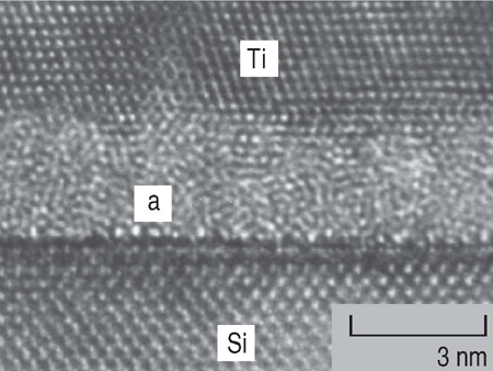
refractory metal/silicon systems.811
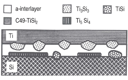
In the Ti/Si system, Ti5Si3, located at
the Ti/ainterlayer interface was identified to be the first nucleated phase.9 Ti5Si3,
Ti5Si5, TiSi, and C49-TiSi2, along with
an amorphous interlayer, were observed
to be present simultaneously in samples
annealed at higher temperatures.10
Examples are shown in Figures 2 and 3. Similar results were obtained for many
refractory metal-silicon systems.8 For the
near-noble silicides, a complex formation
sequence was also found recently.
The complex sequence of nickel silicide
formation has been observed with the
sheet resistance measurements combined
with in-situ x-ray and light-scattering
measurements in a synchrotron radiation
facility.5
Growth Kinetics of Silicides
Kinetic data are crucial for a basic
understanding of interfacial reactions
between metal thin films and silicon.
Most silicides are formed at a temperature
far lower than the eutectic
temperature. The growth is often diffusion
controlled or interface-reaction
controlled. The thickness of the silicide
is proportional to the square root of
time t and t, respectively. The presence
of contaminating or doping impurities
was found to influence the growth rate.
For platinum films deposited in ultrahigh
vacuum, the growth rate of PtSi was
found to increase significantly. However,
the growth law remained the same.12
Cross-section transmission electron
microscopy (XTEM) has been demonstrated
to provide direct and accurate
kinetic data, such as the sequence of
phase formation, the dependence of the
phase growth, and morphology of phase
and interface structure in the growth of
silicides on silicon.13
In TiSi2, CoSi2, NiSi2, and a number
of RE silicides, the silicide formation
took place within a narrow temperature
range and nucleation was suggested as
a controlling mechanism.14 The nucleation
effects are eliminated when these
phases are formed on an amorphous
layer.15 The importance of nucleation
effects in silicide formation has been
discussed extensively by dHeurle.14 The
films produced from nucleation-limited
reactions are often rather rough.
Dominant Diffusing Species
In the silicide formation, metal
atoms diffuse across the metal/silicide
interface, silicon atoms diffuse across
the silicide/silicon interface, or both. In
order to determine the dominant diffusing
species, it is common to introduce an
inert marker. In thin film reactions, the
markers are usually tens of nanometers in
size and should not influence the growth
kinetics of silicide formation. Ideally,
the markers should be inert and remain
immobile as the diffusing species streams
by. An additional constraint is that the
marker should be located in the silicide
layer to avoid possible influence due to
the presence of the interface.7
From the marker experiments, it was
revealed for metal-rich silicides such as
M2Si, the dominant diffusing species are
mostly metal atoms. On the other hand,
in the formation of monosilicide and
disilicide, silicon atoms are generally
the dominant diffusing species. However,
there are exceptions. Important silicides
in ultralarge-scale integrated-circuit
technology, the dominant diffusing
species in the growth of TiSi2, CoSi2,
WSi2, and NiSi are Si, Co, Si, and Ni,
respectively.6,7,14 For the TiSi2 salicide
process, if the temperature, time, and
ambient for the rapid thermal annealing
were not optimized, C49-TiSi2 and/or
C54-TiSi2, which are not easily removed
by ammonia and peroxide solution, are
prone to form on the dielectric sidewall
between the poly-gate and source/drai.
This results in the so-called bridging
problem, which may lead to device
failure. Since cobalt is the dominant diffusing
species in the formation of CoSi2,
the bridging problem is less troublesome
in the CoSi2 salicide technology.
Epitaxial Growth of Silicides
Epitaxial silicides belong to a special
class of silicides that exhibit a definite orientation
relationship with respect to the
silicon substrate. A silicide is expected to
grow epitaxially on silicon if the crystal
structures are similar and the lattice
mismatch between them is small. The
impetus for the study of epitaxial silicides
mainly stemmed from several favorable
characteristics of epitaxial silicides in
comparison with their polycrystalline
counterparts, including greater stability
and a lower stress at the interface,
alleviation of grain boundary effects, as
well as conductivity enhancement.16
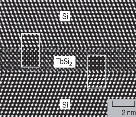
NiSi2 and CoSi2 can be grown in
single-crystal form on silicon.17 Many
hexagonal RE silicides have been grown
on Si(111) for the almost perfect lattice
matches between RE silicide (0001) and
Si(111) planes. Furthermore, on top of
the silicide layer, a single-crystal silicon
layer can be grown. An example of the
Si/TbSi2/Si heterostructure is shown in
Figure 4.18 On the other hand, almost all
transition metal silicides can be grown
epitaxially on silicon to a certain extent.
In particular, FeSi and TiSi2 can be
grown to tens of micrometers in grain
size.16
Initial studies on the epitaxial growth
of silicides on silicon were mostly on
the growth of silicides on a large area.
However, in device applications, silicides
were grown on laterally confined silicon.
Lateral confinement was found to exert
significant influence on the epitaxial
growth of NiSi2 and CoSi2 on silicon.1921
The epitaxial silicides were relevant to
the device applications as the contact
size shrank to sub-100 nm.
In an Ni/(001)Si system, low-resistivity
NiSi is at the center of attention in
device applications. In nickel on blank
(001)Si, NiSi is formed and stable at 350700°C.6 It has been reported that dopants
do not affect NiSi formation.22 However,
striking effects of B+ and BF2+
implantation
on the growth of epitaxial NiSi2 on
silicon were observed. As a result of ion implantation into (001)Si, epitaxial NiSi2
was found to grow at 200280°C instead
of the usual formation temperature of
about 800°C on blank (001)Si. Both
boron and fluorine atoms introduced by
ion implant into silicon were found to
promote the epitaxial growth of NiSi2 on
silicon at low temperatures. Good correlation
was found between the atomic
size factor and the resulting stress and
NiSi2 epitaxy at low temperatures. The
final structure of the silicide layer was
found to depend critically on the thickness
of the starting nickel overlayer
and the annealing temperature. The
amorphicity of the substrate apparently
played an important role in promoting
the formation of polycrystalline NiSi2 at
low temperatures.2325
NANOSILICIDES
Nanoscale silicides are named nanosilicides.
As the integrated circuit industry
moves into the nano-era, metal silicide
contacts are naturally falling into this
category. On the other hand, many efforts
have been made to fabricate nanosilicides
employing the bottom-up approach
without elaborate microlithography.
Nanodots
Quantum dots are envisioned to be
useful in devices such as single-electron
transistors, high-density memories, light
emission, semiconductor lasers, and
tunnel diodes.26 In principle, any ultrathin
(~ 1 nm) silicide forming metal film may
react with silicon substrate to form silicide
nanodots under appropriate annealing
conditions. Other means, such as ion
implantation of metal ions into silicon
nanowires followed by annealing, may
also produce silicide nanoparticles.27 To
meet the requirements of microelectronics
and optoelectronics, it is imperative
to control the size, density, and ordering
of the dots.
Self-assembly is an attractive nanofabrication
technique because it provides
the means to precisely engineer
structures on the nanometer scale over
large sample areas. Self-organizing
nanocrystal assemblies have already
shown the degree of control necessary
to address the challenges of building
nanometer-scale technologies.28
Self-Assembled Low-Resistivity
Metal Silicide Quantum Dot
Arrays on Epitaxial Si0.7Ge0.3
on (001)Si
Si1xGex/Si heterostructures are used
to fabricate high-speed transistors that
extend the range of applications of silicon
technology.29 Self-assembled NiSi
quantum-dot arrays have been grown on
relaxed epitaxial Si0.7Ge0.3 on (001)Si.
The formation of the one-dimensional
(1-D) ordered structure is attributed to
the nucleation of NiSi nanodots on the
surface undulations induced by step
bunching on the surface of SiGe film.
This results from the miscut of the wafers
from normal to the (001)Si direction.
The two-dimensional (2-D), pseudohexagonal
structure was achieved under
the influence of repulsive stress between
nanodots. Since the periodicity of surface
bunching can be tuned with appropriate
vicinality and misfit, the undulated
templates promise to facilitate the growth
of ordered silicide quantum dots with
selected periodicity and size.30
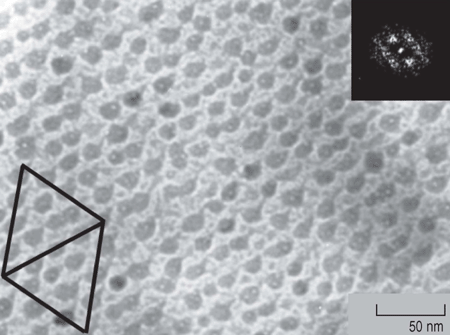
Figure 5 shows a planview TEM
micrograph of an Ni(2 nm)/a-Si(2 nm)/
Si0.7Ge0.3 sample revealing the ordered,
equally spaced NiSi dot arrays, oriented
along the [110] surface direction. The
apparent 1-D alignment and less ordered
2-D arrangement features rule out the
direct influence of the misfit-dislocation
strain. The average size of nanodots and
spacings between adjacent arrays are
about 15 nm and 2040 nm, respectively.
In contrast, NiSi nanodots in Ni/a-Si/
Si(001) samples were found to be randomly
distributed. It indicated that the
use of an Si0.7Gex/Si heterostructure
template induces the highly ordered
alignment of NiSi dots.
A close look at the Si0.7Ge0.3/(001)Si
and Ni(2 nm)/a-Si(2 nm)/Si0.7Ge0.3 surfaces
with HRTEM indeed revealed the presence of the atomic steps, about 520
nm in spacing and 10 nm in average
spacing. The HRTEM images further
showed that the irregularity in step spacing
indicating the presence of step
bunching. In a particular instance, the
nanodot arrays, about 100800 nm apart,
were found to align with the cross-hatch
pattern in a 500°C annealed Ni(7 nm)/a-
Si(13 nm)/Si0.7Ge0.3 sample, as shown in
Figure 6. The nanodots tended to be
connected along individual arrays. The
alignment of nanodots is apparently
under the influence of the strain fields
associated with the cross-hatch patterns.
It is conjectured that the alignment with
the cross-hatch pattern is most prominent
in places where step bunching is of low
density and exerts weak influence on the
formation of nanodot patterns. Similarly,
CoSi2 and TiSi2 nanodot arrays were
formed.31
Formation of Epitaxial β-FeSi2
Nanodot Arrays on Strained Si/
Si0.8Ge0.2 (001) Substrate
Epitaxial β-FeSi2 nanodots were
grown on strained Si/Si0.8Ge0.3 (001)
substrates by the solid-phase epitaxy
method. High-quality β-FeSi2 nanodots
were grown at 800°C by employing
strained Si/Si0.8Ge0.2 substrates, owing
to a decrease of the in-plane lattice
mismatch between the lattice spacing of
the β-FeSi2 [001] and [010] directions
and that of a silicon substrate. Ordered
β-FeSi2 arrays along <110> direction
were observed to form on surfaces of
strained Si/Si0.8Ge0.2 substrate. It is shown
that dislocation slip originating from
compositionally graded Si1xGex layers
can produce local surface-strain and local
thickness variation. The surface features
are used for the fabrication of epitaxial
β-FeSi2 nanostructures on strained Si/Si0.8Ge0.2 substrate.32
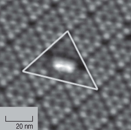
First Nucleated Phase and the
Dominant Diffusing Species
Atomic resolution techniques have
been successful in studying nanoscale silicides.
A particularly pertinent example
is seen in the identification of Ti5Si4 as
the first nucleated phase in submonolayer
titanium deposited on the Si(111)-7×7
surface by ultrahigh vacuum scanning
tunneling microscopy in conjunction
with atomic-resolution TEM. The direct
observation of the formation of clusters
surrounded by the heavily damaged
silicon lattice strongly suggested that
silicon is the dominant diffusing species
in forming the silicide. An example is
shown in Figure 7.33
Nanowires
One-dimensional building blocks,
such as nanowires and nanotubes, are
especially attractive candidates around
which to develop a bottom-up paradigm
for nanotechnology-enabled architectures.
As opposed to zero-dimensional
nanocrystals, which have been the subject
of intense study but are challenging
to contact electrically, nanowires and
nanotubes can act both as interconnects
for the transport of charge carriers as well
as active device elements.34,35 Nanowires
are intrinsically suitable as highly sensitive
sensor elements, due to their high
surface/volume ratio and the extreme
sensitivity of 1-D transport to gating
fields or adsorbates.
Self-Assembled Nanowires
Self-assembled silicide nanowires are
envisioned to possess advantages of
perfect single crystallinity, metallic
resistivity, compatibility with silicon
device processing, and high thermal
stability. A large number of self-assembled
epitaxial silicide nanowires were
investigated in the past.3644 Many RE
silicide nanowires were grown on silicon
substrates. These RE nanowires are
commensurate with nearly perfect lattice
match in their long direction and are
limited in their ability to grow coherently with the substrate in the lateral direction).
For PtSi on Si(001), the long direction
is aligned with [001]PtSi direction in
parallel with the Si(220) plane with
smaller lattice mismatch.45 On the other
hand, for the growth of C49-TiSi2, the
range of structural variants argues against
a simple interface-energy explanation.40
It is, however, interesting that TiSi2
nanowires are incommensurate (8%) in
their long direction.46 However, the
interface structure for the nanowires may
not be the same as that inferred from the
bulk lattices.
|
"The self-assembly of nanowires usually requires that the substrate be crystalline, precluding their use for many potential applications." |
|
For systems of isotropic lattice mismatch,
such as Ni/Si and Co/Si systems,
the aspect ratio of nanowires in these
systems was generally small and unsatisfactory
for practical applications.4244
Strained epitaxial layers may form while
the interface between the overlayer and
the substrate is commensurate. These
layers are inherently unstable and have
interesting properties, which are of
importance in semiconductor devices.
Two kinds of strained relief mechanism
were recognized: one is the formation
of dislocations and the other is shape
transition.
In recent years, it has been recognized
that shape changes such as island formation
constitute a major mechanism for
strain relief.42,47,48 Tersoff and Tromp
reported that a strain-induced shape
transition may occur. Below a critical
size, islands have a compact symmetric
shape. For larger sizes, they adopt a long
thin shape that allows better elastic
relaxation of the islands stress.47
Experimental data on silicide island
formation [e.g., Au4Si/Si(111)48 and
CoSi2/Si(100)]48 also exhibited the elongated
island growth. For the Ti/Si system,
a series of phase transformations was
reported in thin-film reactions.49 Titanium
silicide islands of various shapes
were observed.50 The shapes were found
to depend on the thickness of titanium
deposition and the thermal treatment
process. A previous work showed that
the formation of CoSi2 nanowires
involved the mechanism of endotaxy.44
The twinning relationship with the substrate
breaks the symmetry of the surface
and leads to the asymmetric growth of
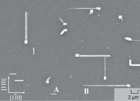
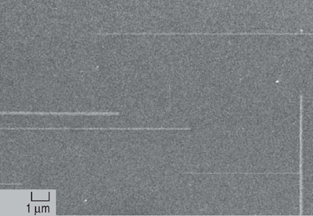
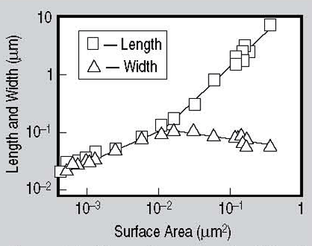
islands. By combining the methods of
reactive deposition epitaxy and nitridemediated
epitaxy, the formation of high aspect
ratio NiSi2 nanowires can be
achieved. Examples are shown in Figures
8 to 10.51 The nanowires were successfully
grown with high aspect ratios
despite the four-fold symmetric epitaxial relationship between NiSi2 (of
cubic CaF2 structure) and silicon (of
diamond cubic structure). Nitride-mediated
epitaxy was presented by Chong et
al. to complement the use of oxide mediated
epitaxy in promoting epitaxial
growth of CoSi2 on (001)Si.52,53 The thin
amorphous interlayer acts as a physical
barrier to control the flux of metal atoms
on the silicon substrate. Such a concept
was used in the growth of self-assembled
silicide nanowires to control the kinetic
process during the growth. A similar
effect is expected to be applicable to
other strained epitaxial layer systems.
The challenges for self-assembled
silicide nanowires are the control of
aspect ratio and location. In addition, the
self-assembly of nanowires usually
requires that the substrate be crystalline,
precluding their use for many potential
applications.
Alternative Growth of Silicide
Nanowires
Alternative approaches have been
adopted to grow nanowires without
relying on the mismatch between the
nanowires and the substrate.
Wu et al. prepared single-crystal
metallic NiSi nanowires using free-standing
silicon nanowires as the template.
NiSi nanowires were produced by
annealing the nickel-metal-coated silicon
nanowires at 550°C. They also prepared
NiSi/Si nanowire heterostructures with
NiSi formed using crossed Si/SiO2 core-shell
nanowires as masks to define the
lengths of the unreacted silicon regions.
Electrical measurements show that the
single-crystal nickel silicide nanowires
have ideal resistivities of about 10μΩcm
and remarkably high failure current densities.
In addition, the nickel silicide/silicon
(NiSi/Si) nanowire heterostructures
have been used to produce field-effect
transistors in which the sourcedrain
contacts are defined by the metallic NiSi
nanowire regions.33 On the other hand,
carbon-coated NiSi nanowires were
prepared in a radio-frequency-induction
heating chemical vapor deposition reactor.
The growth of the NiSi nanowires
and the coating of the nanowires with
carbon layers simultaneously took place
in the reaction. The nanowires were more
than 10 μm long and with an average
diameter of 2040 nm. The resistivity of
individual NiSi nanowire was about 370μΩcm at room temperature, indicating
the presence of considerable impurities
and/or defects.54 Nickel silicide
nanowires were also grown on nickel
surfaces by decomposition of silane at
320420°C. Depending on the growth
conditions, single-phase Ni2Si, Ni3Si2,
and NiSi nanowires were formed. It has
been demonstrated that directed growth
of silicide nanowires can be achieved
with the aid of applied electric field.55
Xiang et al. used a vapor-phase deposition
method to grow TiSi2 nanowires on
silicon wafers. Field emission and cathodoluminescence
measurements reveal the potential applications in vacuum
microelectronics.56
TaSi2 nanowires have been synthesized
by annealing FeSi2 thin film and
nanodots grown on silicon substrate in
an ambient containing tantalum vapor.
The TaSi2 nanowires are formed in three steps: segregation of silicon atoms from
the FeSi2 underlayer to form a silicon
base, epitaxial growth of TaSi2 nanodots
on a silicon base, and elongation of the
TaSi2 nanowire along the growth direction.
Strong field emission properties
promise future electronics and optoelectronics
applications.57
ACKNOWLEDGEMENTS
The research was supported by the
Republic of China National Science
Council through grant No. NSC 93-2215-
E-007-011 and Ministry of Education
grant No. 91-E-FA04-1-4.
REFERENCES
1. The International Technology Roadmap for
Semiconductors, 2004 Update, Semiconductor
Industry Association (San Jose, CA: Semiconductor
Industry Association, 2004), http://public.itrs.net.
2. L.J. Chen, editor, Silicide Technology for Integrated
Circuits (London: IEE, 2004).
3. Z. Ma and L.H. Allen, “Titanium Silicide Technology,”
in Ref. 2, pp. 49–76.
4. T. Kikkawa, K. Inoue, and K. Imai, “Cobalt Silicide
Technology,” in Ref. 2, pp. 77–94.
5. C. Lavoie, C. Detavernier, and P. Besser, “Nickel
Silicide Technology,” in Ref. 2, pp. 95–152.
6. K.N. Tu and J.W. Mayer, Thin Films-Interdiffusion
and Reactions, ed. J.M. Poate, K.N. Tu, and J.W. Mayer
(New York: Wiley, 1978), pp. 359–405.
7. M.A. Nicolet and S.S. Lau, Materials Process
and Characterization, ed. N.G. Einspruch and G.R.
Larrabee (New York: Academic, 1983), pp. 329–464.
8. L.J. Chen, “Solid-State Amorphization in Metal-Si
Systems,” Mater. Sci. Engineering R, 29 (2000), pp.
115–152.
9. M.H. Wang and L.J. Chen, “Identification of the
First Nucleated Phase in the Interfacial Reactions of
Ultrahigh Vacuum Deposited Titanium Thin Films on
Silicon,” Appl. Phys. Lett., 58 (1991), pp. 463–465.
10. M.H. Wang and L.J. Chen, “Simultaneous
Occurrence of Multiphases in the Interfacial Reactions
of Ultrahigh Vacuum Deposited Titanium Thin Films on
Silicon,” Appl. Phys. Lett., 59 (1991), pp. 2460–2462.
11. J.M. Liang and L.J. Chen, “Auto-Correlation
Analysis for the Determination of the Structure of
Amorphous Interlayers in Ultrahigh Vacuum Deposited
Molybdenum Thin Films on Silicon,” Appl. Phys. Lett.,
64 (1994), pp. 1224–1226.
12. C.A. Crider and J.M. Poate, “Growth-Rates for
Pt2Si and PtSi Formation Under UHV and Controlled
Impurity Atmospheres,” Appl. Phys. Lett., 36 (1980),
pp. 417–419.
13. J.Y. Cheng, H.C. Cheng, and L.J. Chen, “Cross-Sectional Transmission Electron Microscope Study of
Growth Kinetics of MoSi2 on (001)Si,” J. Appl. Phys., 61
(1987), pp. 2218–2223.
14. F.M. d’Heurle, “Nucleation of a New Phase from the
Interaction of Two Adjacent Phases: Some Silicides,” J.
Mater. Res., 3 (1988), pp. 167–195.
15. L.S. Hung et al., “Kinetics of TiSi2 Formation by
Thin Ti Films on Si,” J. Appl. Phys., 54 (1983), pp.
5076–5080.
16. L.J. Chen and K.N. Tu, “Epitaxial Growth of Metal
Silicides on Silicon,” Mater. Sci. Reports, 6 (1991), pp.
53–140.
17. R.T. Tung, “Epitaxial CoSi2 and NiSi2 Thin-Films,”
Mater. Chem. Phys., 32 (1992), pp. 107–133.
18. C.H. Luo, F.R. Chen, and L.J. Chen, “Atomic
Structure of Si/TbSi2-x/(111)Si Double Heterostructure
Interfaces,” J. Appl. Phys., 76 (1994), pp. 5744–5747.
19. C.S. Chang, C.W. Nieh, and L.J. Chen, “Formation
of Epitaxial NiSi2 of Single Orientation on (111)Si
inside Miniature Size Oxide Openings,” Appl. Phys. Lett., 50 (1987), pp. 259–261.
20. J.Y. Yew, L.J. Chen, and K. Nakamura, “Epitaxial
Growth of NiSi2 on (111)Si inside 0.1-0.6 μm Oxide
Openings Prepared by Electron Beam Lithography,”
Appl. Phys. Lett., 69 (1996), pp. 999–1001.
21. J.Y. Yew et al., “Formation of CoSi2 on Selective
Epitaxial Growth Silicon inside 0.1–0.6 μm Oxide
Openings,” Appl. Phys. Lett., 69 (1996), pp. 3692– 3694.
22. T. Morimoto et al., “Self-Aligned Nickel-Mono-Silicide
Technology for High-Speed Deep-Submicrometer
Logic CMOS ULSI,” IEEE Trans. Electron Dev., 42
(1995), pp. 915–922.
23. S.W. Lu, C.W. Nieh, and L.J. Chen, “Epitaxial Growth
of NiSi2 on Ion-Implanted Silicon at 250–280°C,” Appl. Phys. Lett., 49 (1986), pp. 1770–1772.
24. L.J. Chen et al., “The Effects of Implantation
Impurities and Crystallinity on the Formation of
Epitaxial NiSi2 on Silicon at 200–280°C,” J. Appl. Phys.,
62 (1987), pp. 2789–2792.
25. W.J. Chen and L.J. Chen, “Interfacial Reactions in
Nickel Thin Films on BF2+-Implanted (001)Si,” J. Appl. Phys., 70 (1991), pp. 2628–2633.
26. C.B. Murray et al., “Monodisperse 3D Transition-
Metal (Co, Ni, Fe) Nanoparticles and Their Assembly
into Nanoparticle Superlattices,” MRS Bull., 26 (2001),
pp. 985–991.
27. C.P. Li et al., “Metal Silicide/Silicon Nanowires from
Metal Vapor Vacuum Arc Implantation,” Adv, Mater., 14
(2002), pp. 218–221.
28. G.M. Whitesides and B. Grzybowski, “Self-Assembly
at All Scales,” Science, 295 (2002), pp. 2418–2421.
29. C.W. Liu and L.J. Chen, “SiGe Heterostructures,” Encyclopedia of Nanoscience and Nanotechnology,
Vol. 9, ed. H.S. Nalwa (Stevenson Ranch, CA: American
Scientific Publishers, 2004), pp. 775–792.
30. W.W. Wu et al., “Self-Assembled NiSi Quantum-dot
Arrays on Epitaxial Si0.7Ge0.3 on (001)Si,” Appl. Phys. Lett., 83 (2003), pp. 1836–1838.
31. L.J. Chen et al., “Nanostructures on Epitaxial SiGe
Films on Silicon,” Electrochem. Soc. PV, 2004-02
(2004), pp. 241–252.
32. H.C. Chen et al., “Growth of Beta-FeSi2 Nanodots
on Strained Si on Si-Ge,” Thin Solid Films, 461 (2004),
pp. 44–47.
33. H.F. Hsu et al., “Identification of the First Nucleated
Phase in Submonolayer Ti Deposited on Si(111)-7×7
by Atomic Resolution Techniques,” Ultramicroscopy,
100 (2004), pp. 347–351.
34. Y. Wu et al., “Single-Crystal Metallic Nanowires and
Metal/Semiconductor Nanowire Heterostructures,” Nature, 430 (2004), pp. 61–65.
35. J.F. Lin et al., “Signatures of Quantum Transport
In Self-Assembled Epitaxial Nickel Silicide Nanowires,” Appl. Phys. Lett., 85 (2004), pp. 281–283.
36. C. Preinesberger et al., “Formation of Dysprosium
Silicide Wires on Si(001),” J. Phys. D: Appl. Phys., 31
(1998), pp. L43–L45.
37. Y. Chen et al., “Self-Assembled Growth of Epitaxial
Erbium Disilicide Nanowires on Silicon (001),” Appl. Phys. Lett., 76 (2000), pp. 4004–4006.
38. J. Nogami et al., “Self-Assembled Rare-Earth
Silicide Nanowires on Si(001),” Phys. Rev. B, 63
(2001), p. 233305.
39. Y. Chen, D.A.A. Ohlberg, and R.S. Williams,“Nanowires of Four Epitaxial Hexagonal Silicides
Grown on Si(001),” J. Appl. Phys., 91 (2002), pp.
3213–3218.
40. M. Stevens et al., “Structure and Orientation of
Epitaxial Titanium Silicide Nanowires Determined by
Electron Microdiffraction,” J. Appl. Phys., 93 (2003), pp.
5670–5674.
41. W.C. Yang, H. Ade, and R.J. Nemanich, “Shape
Stability of TiSi2 Islands on Si (111),” J. Appl. Phys., 95
(2004), pp. 1572–1576.
42. S.H. Brongersma et al., “Stress-Induced Shape
Transition of CoSi2 Clusters on Si(100),” Phys. Rev.
Lett., 80 (1998), pp. 3795–3798.
43. J.D. Carter, G. Cheng, and T. Guo, “Growth of Self-Aligned Crystalline Cobalt Silicide Nanostructures
from Co Nanoparticles,” J. Phys. Chem. B, 108 (2004),pp. 6901–6904.
44. Z. He, D.J. Smith, and P.A. Bennett, “Endotaxial
Silicide Nanowires,” Phys. Rev. Lett., 93 (2004), p.
256102.
45. K.L. Kavanagh, M.C. Reuter, and R.M. Tromp, “High
Temperature Epitaxy of PtSi/Si(001),” J. Cryst. Growth,
173 (1997), pp. 393–401.
46. H.F. Hsu et al., “Shape Transition in the Initial
Growth of Titanium Silicide Clusters on Si(111),” Jpn.
J. Appl. Phys., 43 (2004), pp. 4541–4544.
47. J. Tersoff and R.M. Tromp, “Shape Transition in
Growth of Strained Islands—Spontaneous Formation
of Quantum Wires,” Phys. Rev. Lett., 70 (1993), pp.
2782–2785.
48. K. Sekar et al., “Shape Transition in the Epitaxial-Growth of Gold Silicide in Au Thin-Films on Si(111),” Phys. Rev. B, 51 (1995), pp. 14330–14336.
49. M.H. Wang and L.J. Chen, “Phase Formation in
Ultrahigh Vacuum Deposited Titanium Thin Films on
(001)Si,” J. Appl. Phys., 71 (1992), pp. 5918–5925.
50. K. Ezoe et al., “Scanning Tunnelling Microscopy
Study of Initial Growth of Titanium Silicide on Si(111),” Appl. Surf. Sci., 130-132 (1998), pp. 13–17.
51. S.Y. Chen and L.J. Chen, unpublished work
(2005).
52. R.K.K. Chong et al., “Nitride-Mediated Epitaxy of
CoSi2 on Si(001),” Appl. Phys. Lett., 82 (2003), pp.
1833–1835.
53. R.T. Tung, “Oxide-Mediated Epitaxy of CoSi2 on
Si(001),” Appl. Phys. Lett., 68 (1996), pp. 3461–3463.
54. K.S. Lee et al., “Anomalous Growth and
Characterization of Carbon-Coated Nickel Silicide
Nanowires,” Chem. Phys. Lett., 384 (2004), pp. 215–218.
55. C.A. Decker et al., “Directed Growth of Nickel
Silicide Naowires,” Appl. Phys. Lett., 84 (2004), pp.
1389–1391.
56. B. Xiang et al., “Synthesis and Field Emission
Properties of TiSi2 Nanowires,” Appl. Phys. Lett., 86
(2005), pp. 243101–243103.
57. Y.L. Chueh et al., “Synthesis and Characterization of
Metallic TaSi2 Nanowires,” unpublished work (2005).
L.J. Chen is Ministry of Education National Chair
Professor of the Department of Materials Science
and Engineering at National Tsing Hua University
in Hsinchu, Taiwan.
For more information, contact L.J. Chen, National
Tsing Hua University, Department of Materials Science and Engineering, Hsinchu, Taiwan, +886-3-573-1166; fax +886-3-571-8328; e-mail ljchen@mx.nthu.edu.tw. |
 Presenting a Web-Enhanced